In recent years, wireless communication, optical fiber communication, and high-speed data network products have been continuously introduced, information processing is speeding up, and wireless analog front-end modularization has put forward new requirements for digital signal processing technology, IC technology, and microwave PCB design, and also for PCB boards and The PCB process puts higher demands on it.
For example, commercial wireless communication requires the use of low-cost plates, a stable dielectric constant (with an εr variation error of ±1-2%), and a low dielectric loss (below 0.005). Specific to the PCB of the mobile phone, it also needs to have multi-layer lamination, simple PCB processing technology, high reliability of the finished board, small size, high integration and low cost. To challenge the increasingly fierce market competition, electronics engineers must compromise between material performance, cost, ease of processing, and reliability of finished boards.
There are many plates available at present, and representative commonly used plates are: epoxy resin glass cloth laminate FR4, polyfluorofluoroethylene PTFE, PTFE glass cloth F4, modified epoxy resin FR4, etc. Special plates such as: satellite microwave transceiver circuit to sapphire substrate and ceramic substrate; microwave circuit substrate GX series, RO3000 series, RO4000 series, TL series, TP-1/2 series, F4B-1/2 series. They are used in different occasions, such as FR4 for mixed signal circuits below 1 GHz, polyfluorofluoroethylene PTFE for multi-layer high-frequency circuit boards, PTFE glass cloth fiber F4 for microwave circuit double-sided, modified epoxy resin FR4 is used for high frequency heads of household appliances (below 500MHz). FR4 sheet is widely used because it is easy to process, low in cost and easy to laminate.
Below we analyze the characteristics of microstrip transmission line, multi-layer lamination process, board parameter performance comparison, etc., and give the PCB board selection scheme for special applications, summarizing the high-frequency signal PCB design points for the majority of electronic engineers. reference.
1, microstrip transmission line transmission characteristicsThe performance indexes of the sheet include a dielectric constant εr, a loss factor (dielectric loss tangent) tgδ, surface finish, surface conductor conductivity, peel strength, heat expansion coefficient, and bending strength. The dielectric constant εr and the loss factor are the main parameters.
High-speed data signals or high-frequency signal transmissions are commonly used in microstrip lines, consisting of a conductive strip attached to both sides of the dielectric substrate and a conductor ground plane, and a portion of the conduction strip is exposed to the air, and the signal is on the dielectric substrate and air. Propagation in these two media causes the phase velocity of the transmission to be different, which produces a radiation component. If the size of the microstrip is reasonably selected, the component is small.
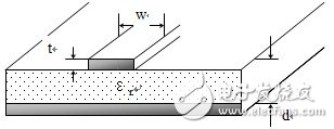
Figure 1 shows the structure of the substrate
As shown in the substrate structure of Figure 1, the copper thickness t is generally small, ranging from 0.5OZ (17μm, 0.7mil) to 1 OZ (35μm, 1.35mil). The conduction band characteristics are substrate dielectric constant εr, line width W. The thickness of the plate is determined.
(1) Microstrip transmission line characteristic impedance
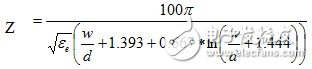
The characteristic impedance Z0 of the microstrip transmission line is calculated as follows: When w/d ≤ 1, the characteristic impedance Z0 of the microstrip transmission line is expressed as:
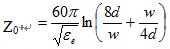
When w/d ≥ 1, the characteristic impedance Z0 of the microstrip transmission line is expressed as:
Where εe is called the effective dielectric constant, which is equivalent to the contribution of the two media to the characteristic impedance of the microstrip as an imaginary uniform medium.
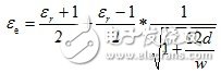
Figure 2 illustrates the relationship between Z0 and W/d, εr. The larger the W/d is, the lower Z0 is, and the larger εr is, the lower Z0 is.
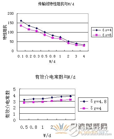
Figure 2 shows the relationship between Z0 and W/d, εr. FR4/S1139 with a thickness of 1.68mm (thickness of the top layer of 0.3mm) provided by Shantou Ultrasonic Printing Board Factory is taken as an example to give a 50 ohm/75 ohm microstrip transmission line width. Parameters, see Table 1.
Dielectric constant εrW / d effective dielectric constant characteristic impedance four-layer board d = 0.3mm eight-layer board d = 10mil
Line width W propagation loss (dB/m) line width W propagation loss (dB/m)
FR44.2~5.4 is subject to 4.8 0.2783.041003mil0.1251 inaccurate
0.7033.24758mil0.12377mil0.1267
1.693.445020mil0.125717mil0.1284
S1139
3.80.392.561004mil0.109
0.8892.737510mil0.110
2.02.9295024mil0.118
Note t thickness is 1OZ/35um/1.37mil
Table 1 50 ohm / 75 ohm microstrip transmission line line width parameters
Also in the design of the six-layer and eight-layer microstrip transmission lines, if the dielectric thickness d of the microstrip line is known, the line width W of the microstrip transmission line can be calculated from the W/d value.
(2) Microstrip transmission line loss
The microstrip transmission line loss is determined by three factors: the radiation caused by semi-openness (this loss is small); the dielectric heat loss αd (plate cause); and the conductor loss αc caused by the high frequency skin effect. Conductor loss is dominant, and conductor loss αc is inversely proportional to W/h (h is the thickness of the substrate) and is also related to the finish. When W/h is constant, the dielectric loss is proportional to the loss factor and frequency.
(3) Microstrip dispersion characteristics
When the frequency is high enough that the microstrip size is sufficiently large relative to λ/4 or λ/2, severe dispersion characteristics will also occur which also increase the radiation loss. If fixed at a certain frequency, the dispersion effect at this frequency may not be considered. The lower the impedance, the thicker the substrate, the higher the εr, the more severe the dispersion of the microstrip, or the higher the frequency, the more severe the dispersion.
(4) Transmission wavelength and phase velocity of the signal in the medium
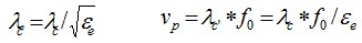
Λc is the actual wavelength of propagation in free space. It can be seen that the higher the εe wavelength is, the shorter the phase velocity of the signal in the transmission line is. The propagation delay t = Vp * L is obtained from the phase velocity and the length of the transmission line.
2, stripline transmission characteristicsThe microstrip transmission line is transmitted in the medium substrate and the air medium, and the strip line is transmitted in the same medium, and has an edge capacitance. The transmission characteristic impedance, loss, propagation wavelength and dielectric material are similar to the microstrip transmission line, and are related to W/b, t/b. Unlike the microstrip transmission line, t has a great influence on the transmission characteristic impedance. Figure 3 shows the stripline transmission. 1.6mm thick, eight-layer PCB board, FR4 board PCB board, its 50 ohm / 75 ohm strip line width parameters are shown in Table 2.
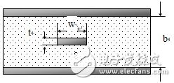
Figure 3 shows the transmission characteristics of the stripline
Dielectric constant characteristic impedance eight-layer board b=16mil line width W propagation loss (dB/m)
FR44.2~5.4
4.8 for reference 505mil0.155
Note t thickness is 1OZ/35um/1.37mil
Table 2 50 ohm / 75 ohm strip line transmission line line width parameters
3, PCB board lamination process and delamination requirements
Parameters such as the total thickness and number of layers of the PCB laminate are limited by the properties of the sheet. Special plates generally have a limited variety of plates of different thicknesses, so designers must rely on plate characteristics and PCB processing limitations in the PCB design process.
FR4 sheet has various thicknesses and is suitable for multi-layer lamination. The table 4 gives FR4 sheet as an example to give a multi-layer laminate structure and sheet thickness distribution parameters for PCB design engineers.
Layer number completes the thickness of the laminate
Four layers 1.5mm2116X2+7628X2+0.8mm
1.57mm7628X4+0.8mm
1.60mm7628X4+0.8mm
1080X2+7628X2+1mm
1.68mm2116X2+7628X2+1mm
Six layers 1.5mm1080X4+7628X2+0.43mmX2
1.6mm1080X4+7628X2+0.43mmX2
Eight layers of 1.5mm1080X6+2116X2+0.27mmX3
1.57mm1080X6+7628X2+0.27mmX3
1.60mm1080X6+7628X2+0.27mmX3
Ten layers of 1.6mm1080X8+2116X2+0.2mmX3
Note 1080 plate thickness 2.5mil /2116 plate thickness 4.3mil / 7628 plate thickness 7mil. The millimeter plate is a double-sided copper plate, and the other is a dielectric substrate. The thickness of the copper skin is 1OZ (35um/1.37mil).
Table 3 FR4 laminate structural parameters six-layer board, completed board thickness of 1.6mm, the laminated structure shown in Figure 4.
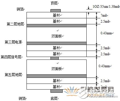
Figure four six-layer laminate structure
4. Comparison of common plate performance parametersFrom the above, the parameters that have the greatest influence on the PCB design and processing of the board are mainly the dielectric constant and the loss factor. For multi-layer board design, the selection of the board also needs to consider punching and lamination performance. The following is a description of the parameters of several types of plates such as FR4/PTFE/F4/S1139/RO4350.
Performance parameter unit plate
FR4S1139RO4350F4 (SGP-500)) PTFE
Dielectric constant 4.2~5.43.83.482.62.5
Loss tangent ≤0.0350.0080.0040.00220.0019
Εr temperature coefficient ppm/0cN/A 50
Thermal expansion coefficient ppm/0c 2114~1621
Copper foil peeling strength pli102.90.92.9
Dimensional stability mm/m 0.5
Difficult to process (hole, surface treatment) and FR4 is equivalent to FR4 when processing through holes, the surface needs special treatment
Comparison of main parameters of Table 3
From the above transmission line characteristic impedance, loss, propagation wavelength analysis and sheet comparison, product design must consider cost and market factors. Therefore, it is recommended that in the PCB design, the designer selects the board to consider the following key factors:
(1) Different signal operating frequencies have different requirements on the board.
(2) FR4 can be selected for PCBs working below 1 GHz, and the cost is low, and the multi-layer press board process is mature. If the signal input and output impedance is low (50 ohms), the transmission line characteristic impedance and the line-to-line coupling need to be strictly considered during wiring. The disadvantage is that different manufacturers and different batches of FR4 plates are doped differently, and the dielectric constant is different (4.2-5.4). Unstable.
(3) Optical fiber communication products operating above 622 Mb/s and small signal microwave transceivers above 1G and below 3 GHz can be modified epoxy resin materials such as S1139, because the dielectric constant is stable at 10 GHz and the cost is relatively high. The low-layer, multi-layer press process is the same as the FR4. Such as 622Mb / s data multiplexing shunt, clock extraction, small signal amplification, optical transceivers, etc. It is recommended to use such panels, in order to make multi-layer board and the board cost is slightly higher than FR4 (about 4 points / cm2) The disadvantage is that the thickness of the substrate is not as complete as the FR4. Or, use RO4000 series such as RO4350, but currently the RO4350 double panel is generally used in China. The disadvantage is that the number of different plate thicknesses of the two plates is not complete, and it is not convenient to make multi-layer printed boards due to the thickness requirements of the plates. For example, RO4350, the plate manufacturer produces four thicknesses of 10mil/20mil/30mil/60mil, and currently has fewer domestic imports, thus limiting the laminate design.
(4) Large-signal microwave circuits below 3 GHz, such as power amplifiers and low-noise amplifiers, are recommended to use double-sided plates similar to RO4350. The dielectric constant of RO4350 is quite stable, the loss factor is low, the heat resistance is good, and the processing technology is equivalent to FR4. The cost of the board is slightly higher than FR4 (about 6 points/cm2).
(5) Microwave circuits above 10 GHz, such as power amplifiers, low noise amplifiers, up-and-down inverters, etc., require higher sheet metal. It is recommended to use double-sided sheets with the same performance as F4.
(6) Wireless mobile phone multi-layer PCB board requires plate dielectric constant stability, low loss factor, low cost, and high dielectric shielding requirements. It is recommended to use plates with properties similar to PTFE (US/Europe, etc.), or FR4 and The high frequency board is combined to form a low cost, high performance laminate.
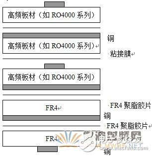
Figure 5 Typical RF/digital multilayer board structure
Typical RF/digital multilayer board structure, based on RO4350 sheet laminate, the possible stripline and microstrip transmission line structure is shown in Figure 5.
5, high frequency board PCB processAccording to the above description of the characteristics of the transmission line, the details of the high-frequency PCB design need to be noted in terms of line width, via, cross-talk, and shielding.
(1) Transmission line width
The transmission line linewidth design is based on impedance matching theory.
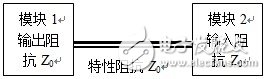
Figure 6 impedance matching
When the input and output impedances and the transmission line impedance match, the system output power is the largest (the total signal power is the smallest), and the ingress and exit reflection is the smallest. For microwave circuits, the impedance matching design also needs to consider the operating point of the device. Signal line vias cause changes in impedance transmission characteristics, and TTL and CMOS logic signal lines have high characteristic impedance, which is not affected. However, this effect of low-impedance, high-frequency circuits such as 50 ohms needs to be considered. It is generally required that the signal line has no vias.
(2) Crosstalk between transmission lines
Coupling occurs when the distance between two parallel microstrip lines is small, causing crosstalk between lines and affecting the characteristic impedance of the transmission line. Special attention should be paid to 50 ohm and 75 ohm high frequency circuits, and measures should be taken in circuit design. This coupling feature is also used in actual circuit design, such as mobile phone transmit power measurement and power control. The following analysis is valid for high-frequency circuits and ECL high-speed data (clock) lines, and for small signal circuits (such as precision operational amplifier circuits).
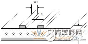
Figure 7. Crosstalk between transmission lines
Let the coupling degree between lines be C, and the size of C is related to εr, W/d, S, and parallel line length L. The smaller the spacing S is, the stronger the coupling is; the longer L is, the stronger the coupling is. In order to increase the perceptual knowledge, for example, a 50 ohm directional coupler made using this characteristic. Such as 1.97GHz PCS frequency base station power amplifier, where d = 30 mil, εr = 3.48:
10dB directional coupler PCB size: S=5mil, l=920mil, W=53mil
20dB directional coupler PCB size: S=35mil, l=920mil, W=62mil
In order to reduce crosstalk between signal lines, it is recommended
A, high-frequency or high-speed data parallel signal line distance S is more than double the line width.
B. Try to reduce the parallel length between signal lines.
C, high-frequency small signal, weak signal avoid strong interference sources such as power supply and logic signal line.
(3) Electromagnetic analysis of grounding vias.
Regardless of whether the IC device pin is grounded or other resistive device is grounded, the ground via is required to be as close as possible to the pin in the high-frequency circuit. The theoretical basis is that the high-frequency signal ground line is equivalent to the ground of the ideal transmission line. The standing wave state is shown in Figure 8.
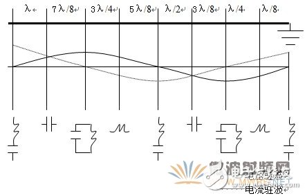
Figure 8 standing wave state diagram
Since the grounding wire is short, the grounding transmission line is equivalent to an inductive impedance (n-pH magnitude), and the grounding via is also approximately equivalent to an inductive impedance, which affects the filtering effect on the high frequency signal. This is why the ground via is as close as possible to the pin. In order to reduce the inductive load of the transmission line, the microwave circuit requires more than one via hole of the grounding pin, which is equivalent to increasing the grounding current capability in the low frequency circuit, and ensuring that each grounding point is equal to 0 level.
(4) Power supply filtering.
In order to reduce the influence of signal logic on the power supply (overshoot), TTL and CMOS circuits add filter capacitors close to the power supply pins. However, it is not enough to take such measures in high-frequency and microwave circuits. The manufacturing process is taken as an example to illustrate the interference of the high frequency signal to the power supply.
Figure 9. The way high frequency signals generate high frequency interference to the power supply
Both of these high frequency signals cause high frequency interference to the power supply and affect other functional circuits. except ![]()
In addition to the power supply pin plus the filter capacitor, the series inductor is also required to suppress high frequency interference. The selection of the series inductance is related to the operating frequency. The basis is that if the power supply pin filters high frequency interference above 1M, where C = 0.1uF, then L = 1uH inductance is selected. Be careful when adding the inductor to the open collector signal pin of the external power supply, because the inductance at this time is equivalent to a matching inductor.
(5) Shielding
Shielding measures are needed in PCB design for small and high frequency signals to reduce large signal (such as logic levels) interference or to reduce electromagnetic radiation from high frequency signals. Such as:
A, digital, analog low-frequency (less than 30MHz) small-signal PCB design, in addition to digital ground and analog ground segmentation, it is also necessary to lay the ground for the small signal wiring area, the ground and signal line spacing is greater than the line width.
B. In digital and analog high-frequency small-signal PCB design, it is necessary to add shielding or grounding isolation measures in the high-frequency part.
C. In high-frequency large-signal PCB design, the high-frequency part needs to be designed with independent functional modules and a shielding box to reduce the external radiation of high-frequency signals. Such as fiber 155M, 622M, 2Gb / s transceiver module.
Multi-layer PCB layout (Nokia 6110), double-sided device, mobile phone PCB design shown in Figure 10.
Figure 10 mobile phone PCB design example
6, plate selection examplesTake the high-frequency (microwave) PCB we designed and debugged as an example to illustrate the selection of the board.
(1) Selection of 2.4 GHz spread spectrum digital microwave relay board
Its structure includes 2M digital interface, 20M spread spectrum despreading, 70M intermediate frequency modulation and demodulation board. We use FR4 sheet, four-layer PCB board, large-area paving, high-frequency analog part of the power supply is insulated from the digital part by the inductor choke.
The 2.4GHz RF transceiver adopts F4 dual-panel, and the transceiver is shielded by metal box and filtered by the power input.
(2) 1.9GHz RF transceiver
Among them, the power amplifier uses PTFE sheet, double-sided PCB board; the RF transceiver uses PTFE sheet and four-layer PCB board. All are made of large-area paving, functional module shield isolation measures.
(3) 140MHz IF transceiver
The top layer is made of 0.3mm S1139 sheet, which is covered with large area and separated by via holes.
(4) 70MHz IF transceiver
FR4 sheet, four-layer PCB board. Large area paving, functional module isolation strips are isolated with a series of vias.
(5) 30W power amplifier
RO4350 sheet, double-sided PCB board. Large area paving, spacing constraint is greater than or equal to 50 ohm line width, shielded with metal box, power input filter.
(6) 2000MHz microwave frequency source
It is made of 0.8mm thick S1139 sheet and double-sided PCB board.
The devices in the wireless field are extensive and the applications are complicated. Especially in the current wireless communication market, the competition is fierce, and the price and time of the products are increasingly becoming the focus of competition. Therefore, the PCB design of electronic engineers can not simply consider the advanced nature of technology, must be considered from many aspects, balance the technological advancement, price advantage and shorten the time to market, and improve the competitiveness of products.
Camping Light Tower,Outdoor Lighting Tower,Manual Type Light Tower,Balloon Metal Halide Light Tower
Wuxi Doton Power , http://www.dotonpower.com