With the rapid development of wireless communication technology and the continuous evolution of specifications in the past ten years, various wireless technologies, such as GSM, GPS, WLAN (such as Wi-Fi), Bluetooth, etc., have gradually emerged and become popular in daily life. in. The wireless communication technology itself is already profound and profound, and when it is introduced into various electronic devices and applications, it is necessary to consider the problems of electromagnetic interference (Electromagne TIc Interference, generally known as EMI) and electromagnetic compatibility (Electromagne TIc CompaTIbility, EMC). Avoid the interference of related functions and cause signal degradation and affect its normal operation. However, although the world has already enacted legislation to establish relevant electromagnetic specifications, focusing on the limitations of electromagnetic radiation and RF (Radio Frequency), it is difficult to have a situation in which different communication modules may interfere with each other. Set a fixed standard to prevent or solve related problems, which has become the most important focus for product developers.
In addition, with the recent boom in portable devices and the diversification of communication functions, these related communication modules and antennas must be designed to be lighter, thinner and shorter, to meet the needs of mobile applications. It is even more difficult to make the product to be optimized. To build more different wireless modules and antennas in extremely small and streamlined spaces, these components are bound to be more susceptible to noise interference and affect their transmission performance, because it is often observed that the transmission distance becomes shorter. The transmission rate is reduced, which is not conducive to the communication performance of the product. In this article, Allion Labs, Inc. will introduce how to correctly measure wireless communication signals and perform electromagnetic compatibility analysis under wireless communication conditions. It is hoped that it can exchange ideas and provide technical references with relevant developers.
Complex communication environment: Receive sensitivity deterioration caused by Platform Noise (De Sense)First, let's first think about the possible situation when the average consumer is using a new handheld device (whether a smart phone or a tablet): when the consumer arrives at the meal time and wants to find a nearby restaurant, he can take out the mobile phone. Click to open a pre-downloaded application, and then voice-activated to say the type of food you want to select. Then, the application will send the received voice to the server of the application provider on the network for interpretation. The user's location and search, and the eligible options and even the map are displayed on the screen, the user can find the right ideal restaurant according to the map.
In fact, in the seemingly simple operation of just a few seconds, there are many components involved in the operation, including the touch screen, the product (hardware) and the user interface (software). The microphone transmits the clean user voice, the activation of the 3G module, the connection capability with the neighboring base station, the role of the GPS positioning system, and the backhaul of the server search result by eliminating the background noise reception. Although the user feels the use of "good and bad", but for the developer, it must be verified from the mechanical structure, component selection, software and hardware integration to the communication module. Create good use experience and fully realize the purpose of using the product.
Therefore, understanding all the components of the product that may generate electromagnetic signals in the entire communication environment is an important prerequisite for the design of the building. Through Figure 1, we can clearly see that there are mainly four types of components in the current new type of devices that generate electromagnetic signals. If the signals emitted by these components are interfered by each other due to poor design, they can be called the stage. Noise (Platform Noise). These four types of components include system platforms (such as central processing unit, memory, power supply), internal and external connector coupling paths (such as various transmission interfaces like USB, HDMI), outsourced platform modules (such as touch Screens, camera lens modules, solid state drives, and other components that are assembled after being purchased from manufacturers) and wireless chipsets/wireless modules (such as Wi-Fi 802.11 a/b/g/n, Bluetooth, GPS), etc. Class components need to be carefully measured and calculated to accurately find the best circuit design and proper overall product construction, avoiding interference with each other and minimizing the risk of all possible problems.
What is the meaning of the Platform Noise Interference? For example, the panel is the largest component of all current control devices, and any signal emitted by the antenna inside the device will hit the panel, and the noise emitted by the panel will also enter the antenna; similarly, the electric wave emitted by the antenna will also It affects each interface; the signals sent by different modules will also become mutual noise, which is called so-called noise interference. When these modules and components are operating at the same time, and the interference cannot be controlled to a certain extent, the phenomenon of "DegradaTIon of Sensitivity" (De Sense) will be generated, which will affect the normal operation of the wireless performance of the device. .
For example, in the same frequency band, when the A mobile phone can receive the signals of 1000 channels, and the B mobile phone can only receive 500 channels, in actual experience, the user will think that the receiving performance of the B mobile phone is not good. Since the antenna, filter, and pre-circuit do not perform particularly badly on any particular channel, in summary, this may be because the B-phone has no design in the design and is interfered by the noise of the stage. The so-called reception sensitivity deteriorates.
It is not difficult to measure the noise interference of the stage. You can choose a clean environment without external interference (such as electromagnetic isolation box), and measure the signal throughput (Throughput) effect of a single wireless module connected to the board. As shown in the yellow line segment of Figure 2, and measuring the signal throughput result of the module built into the product system platform (as shown in the blue line in Figure 2), the comparison between the two will reveal the effect on the product. There is a significant signal degradation in the platform. The difference between the path loss (Path Loss) can be regarded as the interference of the station noise.
It is important to emphasize the notion that the presence of stage noise is unavoidable. It is impossible for us to reduce the noise to zero because the module must be powered through the system and the location of the module will affect adjacent modules. With the interface, there is bound to be noise. However, although the existence of the noise of the stage is inevitable, it can try to minimize the interference without affecting the degree of communication performance, which is why we have to measure the noise and find out the cause of the interference.
However, it is not difficult to measure the noise of the stage noise. However, if you want to verify the source of the noise of the stage and the degree of interference caused by individual sources, you need a very complicated and detailed measurement method, which is definitely a developer. A big challenge. Light is the component that controls the cause and cross-measures the components that can cause interference. It can generate thousands of combinations, such as different communication channels, Bluetooth and Wi-Fi, Wi-Fi and 3G, 3G and GPS. Wait, it is possible that signal loss occurs due to conditions such as co-existence and crosstalk. How to accurately judge the main noise sources through the correct measurement sequence and method, and to automatically measure the time-consuming cross-measurement, is the knowledge.
The primary focus of noise reduction: making a reasonable noise budget (Noise Budget) for modulation
It is known that the interference of the stage noise will cause the reception sensitivity to deteriorate, and it is known how to measure, the next key point is to set the permissible value of the device noise, that is, to formulate a reasonable noise budget (Noise Budget). In order to make the most appropriate adjustments for the device. That is to say, it is known how the wireless communication technology can be demodulated (for example, the deterioration condition of the 3G module is known to be demodulated by the GPS module), and the noise level and Eb/No (system average signal-to-noise ratio) are known. After that, the appropriate noise tolerance is set to correct (not eliminate) the noise interference.
However, such corrections are not a single component correction, but require a series of interlocking verifications and modifications. For example, when the screen of the device interferes with the antenna reception, it is not only the panel itself that is to be modulated, but also the display card behind, the input and output power, the design of the line, the LVDS interface, etc., even the surface of the antenna. The current distribution method needs to be modulated. As can be seen from the simplified diagram of Figure 3, there are many variables that affect the ability of the wireless device to receive signals, and each has a systemic dependency. Therefore, according to the actual stage noise condition, a reasonable noise budget is set, and then the modulation is performed to reduce the noise, which is the key to effectively improve the product quality.
Example Description: Maximum Interference Source - Touch PanelAs mentioned above, the touch panel is the largest component in the new types of devices with touch as the core application, and the corresponding interference problems are generated. Therefore, it is ensured that the noise caused by the stage can be controlled. Within the noise budget, it is naturally the first priority in verification. According to the verification experience of Allion, at present, about 60% of the interference problems in smart phones and tablet devices come from the touch panel, and 70% of them are derived from the IC control chip in the panel. Next, we will The verification points for the touch panel will be explained.
As the name suggests, the touch panel is a touch panel. However, the first interference that the touch panel needs to overcome is not from other modules or interfaces in the same device, but the interference caused by the panel itself. . Including panel electrodes such as Pixel Electrode, Pixel Clock, Storage Capacitor, Line-by-Line Address Back Light Unit, etc. Touch interference.
At this time, it is necessary to measure the voltage at the time of touch, scan and observe the voltage changes at different times and using different touch points to understand the actual stage noise condition, in order to perform appropriate modulation. Basically, the touch scan voltage is about 100~200k, and the screen update rate is five milliseconds (ms) to check all touch points. This low cycle frequency is very easy to cause GPS and SIM. Card interference. Therefore, the touch panel must increase the voltage to solve the panel interference, that is, the sensitivity of the touch sensing is reduced by the micro-amplification, so that the noise of the stage is reduced; in actual measurement, in addition to the precise fixture In addition to the instrument, the time domain (not the frequency) must also be measured to obtain true error rate (BER) data.
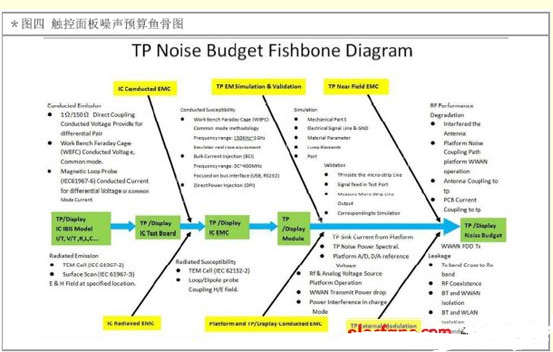
After measuring the noise of the touch panel itself and setting a reasonable noise budget value, the noise measurement of the various touch modules can be started. The touch panel noise budget fish bone of FIG. The graph is the order of measurement and verification that we have summarized based on experience. We must observe the interference of the touch panel on different modules through the control of the noise budget. In the actual measurement chart in Figure 5, the red line is the noise budget we set, and our goal is to reduce the noise value below the red line.
â—LVDS
At present, many new devices such as tablets or Ultrabooks transmit signals in the design panel, so that LVDS is used for transmission. LVDS is Low Voltage Differential Signaling, which is a high-performance and high-performance device. Technology required for low voltage data transmission applications. However, in practical applications, these signals may partially enter the mobile communication band such as 3G, and generate a large ground capacitance imbalance (Ground Capacitance Unbalance) current, and cause interference. However, the traditional treatment method is to alleviate such a situation by attaching a copper foil tape or a conductive cloth, but the actual imbalance of the ground is not solved, and the problem of the LVDS cable is not effectively dealt with. Only by measuring the difference in noise between the closed environment and the system platform of the LVDS signal itself can be adjusted from the source of the problem.
â—Line logic gate
In addition, the touch panel is connected to a number of lines, and the logic gates of these lines will cause frequency interference due to continuous switching. For example, when the logic gate generates about 45MHz of interference, the transmit and receive frequency difference between GSM 850 (869-896 MHz) and GSM 900 (925-960 MHz) is less than 45MHz, and external modulation is generated. Another cause is that the Bluetooth is switched by the logic gate to cause a change in the magnitude of the current. Such external modulation causes the signal to enter the spectrum of GSM1800 and GSM1900 to cause interference.
Therefore, we must use the frequency domain simulation method for S-parameter analysis sampling to confirm that the error values ​​of computer simulation and real machine test are within the allowable range to grasp the noise conduction condition. In order not to sacrifice the good touch experience of the consumer, the interference of the touch panel on other modules and components of the product can be reduced.
â—Solid state hard disk
Emerging storage media - Solid State Drives (SSDs), despite being affected by market price fluctuations in flash memory, remain high in cost, but are widely used in tablets and other forms due to their thin size and low power consumption. In the mobile device. However, the traditional disk-type hard disk is susceptible to external communication conditions (for example, when the mobile phone is placed next to the computer hard disk and may interfere with the hard disk to cause data corruption), it also appears on the SSD.
In the situation on the SSD, the SSD will decrease the noise margin (Noise Margin) with the increase of the number of times of use (P/E Cycle), as shown in Figure 7, after 10,000 times. After smear and use, the noise margin is obviously deteriorated, and it is more susceptible to interference from touch panels or other noise sources, which affects the actual function. In this situation, if the SSD can be evenly smeared, it is one of the methods to effectively reduce the rate of noise margin reduction.
â— Module multitasking operation
The power used by the touch panel comes from the system itself, and other modules such as communication or camera are also powered by the system. Therefore, the stability and sufficient voltage are the key to make these modules work well. Among all the modules that need to use the power supply, especially the 3G or Wi-Fi module is the most power-consuming when connecting online (data transmission). When all these communication modules are turned on, it is likely to cause voltage shortage, which affects The touch panel is stable and eats electricity; in addition, the electromagnetic wave of the communication module may directly hit the panel at the same time, causing serious noise interference. At this time, we must go back to the front of the fishbone diagram, in order to verify the different module settings, location construction, communication environment.
Precise measurement verification can effectively improve communication quality and reduce noise interferenceAt the end of this article, Allion also provides a complete verification step designed by us based on experience, as a reference for development verification. Through such verification sequence, we can reduce noise interference step by step and improve communication quality. According to Figure 8, a complete device with various communication modules and touch functions can be mainly divided into the following three verification steps:
1. Conductive Test:
At the beginning of the verification, the conduction test is required to accurately measure the stage noise of the device itself, the deterioration of the reception sensitivity, and the stage noise at the time of transmission and reception (Tx/Rx).
2. Electromagnetic compatibility (Near Field EMC):
After mastering the relevant information that can be obtained by the conduction test and setting the noise budget, the measurement including the antenna surface current measurement, the noise current distribution measurement and the coupling path loss (Coupling Path Loss), and the camera, The touch panel's noise and RF coexistence are externally modulated.
3. OTA Test (Over The Air Test):
After conducting the conduction and EMC tests, independent and coexisting measurements, total Radiation Power (TRP) and Total Isotropic Sensitivity (TIS) measurements, GPS carrier-to-noise ratio can be performed for different communication modules. (C/N Ratio) measurement and even DVB receiver sensitivity test.
Although the content discussed in this article is only one example of noise verification, we can see the knowledge of wireless communication signal technology and the depth of technology that interferes with control. All relevant business developers need to go through more in-depth research, more technical resources and energy input to find out the corresponding measurement methods and solutions to overcome the communication products. Signal degradation and interference conditions.
Shenzhen Linx Technology Co., Ltd. , https://www.linxheadphone.com