The PIC16F877 has eight 10-bit A/D converters. Pins 2~5 are ANO~AN3 and 7-10 are AN4~AN7.
The MPA-ICD's RAO port on the 16F877 is connected to a 10kΩ potentiometer with voltage, and 8 LEDs are connected to the D port (RDO-RD7), as shown in the figure. One of the 16F877A/D conversion channels is used for A/D conversion to illustrate the method of A/D conversion programming and online debugging and programming.
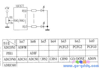
In the figure, the variable output (voltage analog quantity) of R6 is connected to RAO/ANO as an analog input; the 8 LEDs of D port (RDO~RD7) show the result of A/D conversion (displayed in binary) ).
First, the main points of establishing A / D conversion source program
Writing a 10-bit A/D conversion program seems simple, but it is difficult for beginners, because when writing A/D conversion programs, you should be proficient in using multiple special function registers inside the PIC16F877. The table lists some of the special function registers related to A/D conversion.
Register bits not used in the A/D converter are indicated by blanks.
1. A/D pin control register bit 0~bit3 (PCFG0~PCFG3) of ADCONlADCON1 is the A/D conversion function selection bit. If it is 1110, it means that ANO (RAO) channel is analog input, and the other channels are digital I/. O (Other encoding functions, please refer to the book introduction). Bit7 (ADFM) selects the bit for the A/D result format, with 1 indicating a right shift and O indicating a left shift.
2. Bit 6 of the interrupt flag register PIR1PIR1 (ADIF is the A/D interrupt flag bit. This bit is l to indicate that the analog-to-digital conversion has been completed. A value of 0 indicates that the conversion is not completed.
3. A/D operation control register ADCONOADCONO bit0 (ADON) is the A/D conversion enable bit. This bit is 1 to turn on the A/D converter, 0 to turn off the A/D converter; hit2(GO/DONE) is A /D conversion status, this bit is 1 to start A/D conversion, 0 means A/D conversion is completed (this bit is automatically cleared after A/D conversion is completed); bit3~bit5 is A/D channel selection bit The value corresponds to the channel number, ooo is 0 channel; bit6 - Bit7 (ADCSO, ADCSl) is the A/D conversion clock selection, 00:/2osc/2, 01:fosc/8,10:fosc/32,11 :fRC (RC oscillator). For correct A/D conversion, the A/D conversion clock value should not be chosen too small.
4. A/D result The high byte register ADRESH stores the high byte of the A/D conversion result.
The source code for writing A/D conversions also uses the STATUS, OPTION, INTCON-----registers.
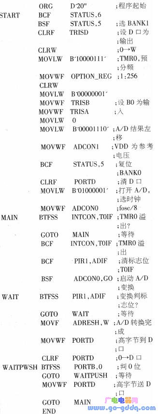
Second, PIC16F877A/D conversion source program. ASM instance
The list of A/D conversion source programs written is as follows:

BAM Power Transmission Capacitors
BAM power transmission capacitors
RAM/RFM Induction Heating Capacitors,Water Pump Capacitor,Water Cooled Condense,Tank Capacitor
YANGZHOU POSITIONING TECH CO., LTD. , https://www.cnchipmicro.com