What is electromagnetic compatibility
Electromagnetic Compatibility (EMC) refers to the ability of a device or system to operate in its electromagnetic environment without causing unacceptable electromagnetic interference to any device in its environment. Therefore, EMC includes two aspects: on the one hand, it means that the electromagnetic interference generated by the equipment in the normal operation of the equipment cannot exceed a certain limit; on the other hand, it means that the equipment has certain electromagnetic interference in the environment. Degree of immunity, ie, electromagnetic susceptibility.
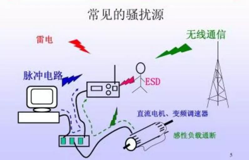
Electromagnetic interference source type
There are many kinds of electromagnetic interference sources and they can be classified according to different methods. The sources of interference that directly affect the measurement and measurement equipment in the measurement environment can be divided into natural and artificial interference sources.
Natural sources of interference include:
(1) Atmospheric noise interference: such as spark discharge generated by lightning, is pulsed broadband interference, which covers from several Hz to 100MHz or more. The spread is quite far.
(2) Solar noise: It refers to the radiation noise of sunspots. During the sunspot activity. The explosion of sunspots. It can generate thousands of times more intense noise than the stationary phase. Causes the communication to be interrupted.
(3) Ning Zhou noise: refers to the noise from the universe.
(4) Electrostatic discharge: Electrostatic voltage accumulated on the human body and equipment can be as high as tens of thousands of volts up to hundreds of thousands. Often discharged by corona or sparks, called electrostatic discharge. Electrostatic discharges generate powerful transient currents and electromagnetic pulses that can damage static-sensitive devices and devices. Electrostatic discharge is a pulse broadband interference, spectrum components from the DC has been continuous sword frequency band.
Sources of human interference refer to electromagnetic interference generated by electrical and electronic equipment and other artificial devices. The man-made interference sources mentioned here refer to unconscious interference. As for the intentional release of interference in order to achieve a certain purpose, such as electronic countermeasures, etc. are beyond the scope of this article.
Any electronic and electrical equipment may cause human interference. Here, only some common interference sources in the interference measurement environment are mentioned.
(1) Radio transmission equipment: including mobile communication systems, radio, television, radar, navigation and radio relay communication systems. Such as microwave relays, satellite communications, etc. Due to the large power emitted, its fundamental signal can produce functional interference; harmonics and spurious emissions constitute non-functional unwanted signal interference.
(2) Industrial, scientific, medical (ISM) equipment: such as induction heating equipment, high-frequency welding machine, X-ray machine, high-frequency physiotherapy equipment, etc. The powerful output power not only interferes with the radiation of space, but also interferes with remote devices through the power frequency network.
(3) Power equipment: Including servo motors, drills, relays, elevators, etc. The drastic changes in the current generated by the switching on and off of the equipment and accompanying sparks become sources of interference: non-linear loads in the power system (eg, electric arc furnaces, etc.), intermittent power supplies ( UPS) Equivalent power conversion equipment generates a large amount of harmonic influx into the grid and becomes a source of interference: fluorescent devices such as fluorescent lamps also produce glow discharge noise interference.
(4) Ignition systems for automobiles and internal combustion engines: Vehicle ignition systems produce broadband interference, and the interference intensity is almost constant from several hundred kHz to several hundred megahertz.
(5) Grid interference: refers to the interference generated by the powerful electromagnetic field and earth leakage current of the 50Hz AC grid, and the micro arc caused by the poor contact of the high-voltage transmission lines such as corona and insulation fracture, and the spark of the surface of the contaminated conductor.
(6) High-speed digital electronic equipment: Includes computers and related equipment.
The mechanism of the electromagnetic interference source mentioned above is: discharge noise (lightning, electrostatic discharge, glow discharge, etc.). Contact noise, circuit transitions, electromagnetic wave reflections, etc. The reflection of electromagnetic waves in transmission lines is a source of interference that must be taken seriously for high frequency measurements and digital equipment.
Electromagnetic interference hazards:
Interfere with the watching of the TV and listening to the radio.
Loss of data during the digital system and data transmission.
A broken ring that works properly at the device subsystem or system level.
The work of medical electronic equipment is erratic.
The automation of the microprocessor control system is out of control.
The navigation system is malfunctioning.
Unexpected explosion of the detonation device.
Failure of industrial process control functions.
In addition to the strong electric field will also affect the organism, generally can be divided into thermal effects and non-thermal effects. For thermal effects, as the radio frequency incident power density gradually increases, localized body temperature may increase, blood activity may be increased at sites with less blood distribution, enzyme activity may be reduced, egg degeneration, heart rate changes, or even thermoregulatory capacity may be suppressed. Impaired until death. For non-thermal effects, the impact is extensive. Including the impact on the central nervous system, blood immune system, cardiovascular system, reproductive system and embryonic development. These effects not only reflect the individual level, but also affect the cell level.
Electromagnetic Compatibility Design Requirements
Requirements for electromagnetic compatibility design:
1 clear system electromagnetic compatibility indicators. Electromagnetic compatibility design includes the electromagnetic interference environment in which the system can maintain normal operation and the allowable indicators of other systems that the system interferes with.
2 Based on the understanding of the sources of interference, the objects to be interfered with, and the interference paths of the system, these indicators are gradually distributed to sub-systems, subsystems, circuits, components, and devices through theoretical analysis.
3 According to the actual situation, take appropriate measures to suppress the interference source, eliminate the interference, and improve the circuit's anti-jamming capability.
4 Through experiments to verify whether the original set of indicators has been met, if not, then take further measures, repeated several times until it reaches the original target.

EMC main research object
1 Various kinds of man-made noise, such as transmission line corona noise, car noise, contactor noise itself, and noise caused by discharge when the conductor starts, electric locomotive noise, urban noise, etc.
2 The mutual influence of various public utilities (power lines, communications, railways, highways, oil and metal pipelines, etc.) in the shared corridor.
3 Reflection problems caused by large buildings such as super high-rise buildings, transmission lines, and iron towers.
4 The role of the electromagnetic environment on humans and all kinds of organisms. These include power frequency fields such as strong wires, medium and short-wave and microwave electromagnetic radiation.
5 nuclear electromagnetic pulse effects. Electromagnetic pulses from high-altitude nuclear explosions can destroy large areas of command, control, communications, computers and newspaper systems on the ground.
6 TEMPEST technology. Its substantive content is aimed at the problem of electromagnetic radiation and information leakage of information equipment, and a series of research work carried out from the aspects of information reception and protection.
7 Misoperation of electronic equipment. In order to prevent malfunctions, measures must be taken to improve the anti-jamming capability of the equipment.
8 spectrum allocation and management. The radio spectrum is a limited resource, but it is not expendable. It must be managed scientifically and fully utilized.
9 Electromagnetic Compatibility and Measurement.
10 natural influences and so on.
Basic method of electromagnetic compatibility measurement
1, electromagnetic radiation emission measurement system
Electromagnetic field radiation measurement is the measurement of electromagnetic radiation intensity of electrical and electronic equipment
2. Electromagnetic radiation sensitivity test system: its measurement methods mainly include the following
1) Generate a disturbing electromagnetic field with a transmitting antenna,
2) Generate harassing electromagnetic fields with a TEM cell or GTEM cell,
3) Generate a harassing electromagnetic field with the reverberation room,
4) Use Helmholtz coils to generate magnetic fields
3, conductive emission measurement system: There are the following methods of measurement
1) Stability of network LISN through line impedance
2) Use a current probe to measure the interference power on the power line.
3) Measure the interference power on the power line through the power absorption clamp
4, Conductivity Test System: There are several ways to enter the interference signal
1) Pass the transformer into the measured line to enter the interference signal,
2) Incoming interference signals to the measured line through the coupling/decoupling network,
3) Inject interference signals into the measured line by injecting the probe.

Measures to improve electromagnetic compatibility
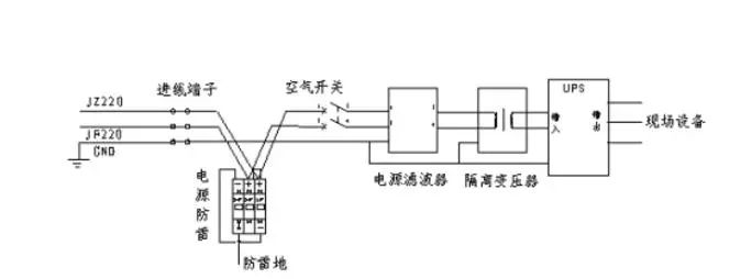
1 The use of a complete shield can prevent external radiation from entering the system and can also prevent the system's interference energy from radiating outward. The shield body should maintain its integrity. The necessary doors, slots, ventilation holes, and cable holes must be properly handled. The shield body must be grounded reliably.
2 Design a reasonable grounding system. Small-signal, large-signal, and interference-prone circuits should be grounded as closely as possible. The grounding resistance should be as small as possible.
3 Using appropriate filtering techniques, the filter's passband is properly chosen to minimize leakage losses.
4 Using clipping techniques, the slice level should be higher than the working level and should be bi-directionally limited.
5 Select the correct connection cable and wiring method. If necessary, replace the long cable with fiber optic cable.
6 using balanced differential circuit, shaping circuit, integrator circuit and strobe circuit technology.
7 system frequency allocation should be appropriate. When there are multiple main frequency signals working in a system, try to avoid the frequency of each signal, and even avoid the other party's resonant frequency. 8 The equipment in the shared corridor should be kept at a larger gauge when the conditions permit so as to reduce the mutual influence.
Electromagnetic Compatibility Course Features
1. Electromagnetic compatibility is based on electromagnetic theory. Therefore, the principle of electromagnetic compatibility is based on the theory of electromagnetic fields.
2. Electromagnetic compatibility is a comprehensive edge discipline. Therefore, mastering electromagnetic compatibility requires a multidisciplinary knowledge base.
3, electromagnetic compatibility is more practical. Therefore, to master and use electromagnetic compatibility technology flexibly requires designers to constantly practice and accumulate experience.
4, a lot of reference to the concept and terminology of radio technology.
5, the particularity of the unit of measurement. The most commonly used unit of measurement in electromagnetic compatibility engineering is decibel (dB)
EMC implementation
1. Power supply: Since many electromagnetic interferences are coupled to the electronic device through the power supply, special electromagnetic compatibility design is performed on the system power supply. Increase effective transformer, regulator, and filter circuits, use high-efficiency switching power supply chips and low-dropout linear power supply chips with good voltage regulation and filtering to provide a stable and reliable power supply for the system.
2. Use decoupling capacitors: Add a decoupling capacitor between each power supply of the integrated circuit and ground. The decoupling capacitor has two functions: on the one hand, the storage capacitor of the integrated circuit provides and absorbs the charge and discharge energy of the integrated circuit for opening and closing the door; on the other hand, it bypasses the high-frequency noise of the device.
3. Ground separation: The use of 4-layer circuit board design to reduce the parasitic inductance of the power supply and ground effectively enhances the EMC performance of the system. A separate power layer and ground layer can effectively prevent the devices from being coupled to each other through the ground line and the power supply. In addition, the method of splitting and isolating the ground lines with different properties enables the currents of different attributes of the ground lines to go through different paths and prevent Signal crosstalk.
Communication interface: The system's 485, 232, USB and other communication interface external cables, and has direct contact with external devices, so it is also vulnerable to various electromagnetic interference, in order to enhance the anti-interference ability of these communication interfaces, in the communication signal line Magnetic beads and shunt varistors, as well as filter capacitors;
In addition, in order to enhance the noise immunity and reduce the degree of harassment, the following principles should be followed when laying out the PCB board:
1. The quartz crystal oscillator should be as close as possible to the device that uses this clock. The clock line should be as short as possible. The housing should be grounded. Use the ground wire to circle the clock area.
Do not route under quartz crystals and under noise-sensitive devices.
2. The I/O driver circuit should be as close to the printed board as possible, allowing it to leave the printed board as soon as possible. The signal entering the printed circuit board must be filtered, the signal from the high noise area must be filtered, and the signal reflection can be reduced by using the series termination resistor.
3. MCU useless terminal must be connected high, or grounded, or defined as the output terminal, the end of the integrated circuit should be connected to the power supply, do not float. Don't leave unused gates unconnected.
4. The printed board should use 45 fold lines instead of 90 fold lines to reduce the external emission and coupling of high frequency signals.
5. Correctly select single-point grounding and multi-point grounding. In the low-frequency circuit, the operating frequency of the signal is less than 1MHz, and its influence on the inductance between the wiring and the device is small, and the circulation current formed by the grounding circuit has a great influence on the interference, so a point should be grounded. When the operating frequency of the signal is greater than 10 MHz, the impedance of the ground wire becomes very large. At this time, the resistance of the ground wire should be reduced as much as possible, and the multi-point grounding should be used nearby. When the operating frequency is from 1 to 10 MHz, if a point is grounded, the length of the ground wire should not exceed 1/20 of the wavelength. Otherwise, the multi-point grounding method should be adopted.
6. Separate the digital circuit from the analog circuit. There are both high-speed logic circuits and linear circuits on the circuit board. They should be separated as much as possible, and the ground lines of the two should not be mixed. They are connected to the power supply ground. Try to increase the grounding area of ​​the linear circuit.
7. Make the ground wire as thick as possible. If the grounding wire is very fine, the grounding potential changes with the change of the current, causing the timing signal level of the electronic equipment to be unstable and the anti-noise performance to deteriorate. Therefore, the ground wire should be as thick as possible so that it can pass three times the allowable current of the printed circuit board. If possible, the width of the ground wire should be greater than 3mm.
8. Make the ground wire a closed loop. When designing a printed circuit board ground system consisting of only digital circuits, making the ground wire a closed loop can significantly improve the noise immunity. The reason lies in the fact that there are many integrated circuit components on the printed circuit board, especially when there are many components that consume more power, due to the limitation of the thickness of the grounding wire, a large potential difference will be generated in the ground junction, resulting in a decrease in the anti-noise ability. If the grounding structure is looped, the potential difference will be reduced and the anti-noise capability of the electronic equipment will be improved.
9. Choose a reasonable wire width. Because the impact interference produced by the transient current on the printed lines is mainly caused by the inductance components of the printed conductors, the inductance of the printed conductors should be minimized. The inductance of a printed conductor is proportional to its length and inversely proportional to its width, so a short, fine conductor is good for suppressing interference. Clock lines, row drivers, or bus driver signal lines often carry large transient currents. Printed conductors must be as short as possible. For discrete component circuits, when the width of the printed conductor is about 1.5mm, it can fully meet the requirements; for integrated circuits, the width of the printed conductor can be chosen between 0.2~1.0mm.
10. Use the correct cabling strategy. Equivalent traces can reduce the inductance of the wire, but the mutual inductance and distributed capacitance between the wires increase. If the layout allows, it is better to adopt the grid structure of the grid structure. The specific approach is to laterally route one side of the printed circuit board, and the other is to make vertical wiring. Then connect them with metallized holes at the cross holes. In order to suppress the crosstalk between printed circuit board conductors, it is necessary to avoid long-distance equal alignment when designing the wiring.
Shenzhen Chengrong Technology Co.ltd is a high-quality enterprise specializing in metal stamping and CNC production for 12 years. The company mainly aims at the R&D, production and sales of Notebook Laptop Stands and Mobile Phone Stands. From the mold design and processing to machining and product surface oxidation, spraying treatment etc ,integration can fully meet the various processing needs of customers. Have a complete and scientific quality management system, strength and product quality are recognized and trusted by the industry, to meet changing economic and social needs .
Phone Holder Usa,Phone Holder For Car,Iphone 12 Pro Max Stand,Iphone 12 Charging Base
Shenzhen ChengRong Technology Co.,Ltd. , http://www.laptopstandsupplier.com