This article introduces the design of a portable patrol machine (RF reader). The reader is mainly composed of MCU, RF IC card reader module, antenna and USB communication interface. In order to facilitate real-time recording of the patrol situation, the system uses a clock chip with a time reference function.
With the rapid development of smart communities and smart buildings in recent years, the patrol system will have wide application prospects. The main development indicators of handheld readers include miniaturization, low power consumption, portable and convenient data transmission interface.
Reader overall design
Portable IC card readers are mainly powered by batteries. Because the reader continuously emits radio waves and consumes a lot of power, it is necessary to consider how to reduce power consumption from every detail, so as to extend the battery life as much as possible. The hardware uses low-power design, such as low-power devices, low voltage, modular power supply, etc .; the software uses a large-scale design to minimize the working time of the processor and keep it in a low-power operating mode.
The design of the reader must meet the following requirements: it has a self-checking function, which can first check whether the device is faulty when it is turned on; it can accurately and quickly read the information in the non-contact IC card; it has an audible and visual alarm circuit; the battery directly Power supply, can be powered by 3 AA nickel-hydrogen batteries, startup static current is not more than 10mA, working current is not more than 40mA; with USB communication interface; small size, low cost, stable and reliable performance.
System function overview
According to the requirements of the patrol system on different occasions, it is necessary to know the patrol situation of the patrol personnel in time to ensure the safety of the community, shopping malls, and railways.
Therefore, the system should have the following functions: install a series of RF cards representing different points on the determined patrol line, and when reaching each point, the patrol personnel use a hand-held patrol machine to approach the patrol detection point, and put the representative of the point The card number and time are recorded at the same time; after the patrol is completed, the patrol machine stores the collected information in the USB disk through the USB interface chip or directly passes it to the computer software for processing.
System hardware design
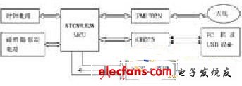
Figure 1 Functional block diagram of a portable RF reader
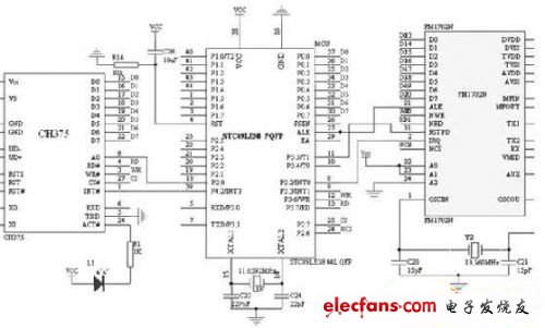
Figure 2 Schematic diagram of the main control module circuit
2 RF module design
The read-write module is a communication medium between the radio frequency IC card and the outside world. The antenna connected to the read-write module resonates with the IC card coil to perform data transmission and complete the communication between the read-write module and the card. The FM1702N used in this design supports TYPE A contactless communication protocol at 13.56MHz. It is the core module for wireless communication with contactless IC cards and a key interface chip. It modulates the data in the transmission buffer according to the design of the register to obtain the transmitted signal, which is sent out in the form of electromagnetic waves through the antenna driven by the TX1 and TX2 pins, and the IC card responds with the load modulation of the RF field. The response signal of the antenna pickup IC card is sent to the RX pin through the antenna matching circuit. The FM1702N internal receive buffer detects and demodulates the signal and processes it according to the settings of the register. The processed data is sent to the parallel interface and read by the MCU.
3 Antenna design
In order to communicate with the non-contact IC card, the reader must have an antenna capable of transmitting and receiving radio frequency signals. Antennas of different sizes and shapes can be designed for different applications. The specific steps of antenna design are: setting the working environment of the reader, optimizing the coupling coefficient between the reader and the transponder, and determining the antenna coil and capacitance.
The non-contact IC card antenna uses inductive coupling to generate magnetic flux, which is used to provide power to the transponder and transfer data between the two. Therefore, there are several basic requirements for the construction of the reader antenna: the maximum current of the antenna coil is used to generate the maximum magnetic flux Φ; the power is matched to maximize the use of the available energy to generate magnetic flux; the bandwidth is sufficient to be free of distortion Carrier signal that transmits data modulation.
4 buzzer drive circuit design
The buzzer sounds an alarm indication sound every time the card reading operation is unsuccessful. Due to the limited driving capability of the I / O port of the MCU, it is generally impossible to directly drive the piezoelectric buzzer, so a PNP type transistor is used to form the transistor drive circuit. The output of the MCU I / O port (P3.4) is amplified by the drive circuit. Can drive the buzzer. This design selects the working current of the buzzer as 10mA, and its driving circuit is shown in Figure 3.
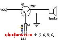
Figure 3 buzzer drive circuit
5 Clock circuit design
The real-time clock is implemented with a low-power CMOS real-time clock / calendar chip PCF8563. PCF8563 provides a programmable clock output, an interrupt output, and a power-down detector. All its addresses and data are serially transferred through the I2C bus interface (by P1 of STC89LE58R) .6 and P1.7 form an analog I2C serial port). The clock circuit mainly collects real-time time for real-time tracking and recording. At the same time, considering that PCF8563 is a real-time clock chip, continuous power supply is still required when there is no external power supply to keep the time accurate. Therefore, this part of the circuit also adds a power-down protection function.
6 Communication interface design
This system uses USB for communication. The USB interface chip uses CH375, which supports HOST host mode and SLAVE device mode. In the USB host mode, CH375 provides both parallel and serial communication methods. In this design, parallel port communication method is used, and D7 ~ D0, RD, WR, A0, CS are directly connected to the MCU through the 8-bit passive parallel interface. On the system bus, the circuit connection is simple. CH375 has built-in firmware that deals with the special communication protocol of mass storage devices, so the MCU of the reader system can communicate with the USB device through the CH375 according to the corresponding USB protocol, and the U disk can be used as a removable mass storage without detailed understanding of USB. Communication protocol, it is possible to read and write data.
System software design
The system software design is mainly divided into three parts, namely the application program design for FM1702N, USB interface program design and main program design.
The reader detects the card after being awakened from sleep. If there is a card or a communication request, it performs normal work processes such as card reading, writing records, and communication. After the work is completed, it enters sleep. If there is no card, it will directly enter the sleep state. The wake-up pulse is fixed once every 500ms. During normal working state, the wake-up interrupt is shielded. Therefore, in the card-free state, the terminal is awakened every 500ms to detect the card. The time of card detection is the main current consumption time, so it is very important to shorten the time of card detection. The system card detection time of this design is 2ms. In this way, the terminal realizes card detection without external intervention, and the power consumption is very low. In the card-free state, in each 500ms cycle, 2 to 3ms are in working state, the transient maximum current is 40mA, and 497 to 498ms are in sleep state, the current is only a few microamperes, and the overall average current is 50μA, so as to achieve Low power consumption requirements for handheld terminals.
MCU uses C51 language programming, the system software flow chart is shown in Figure 4.
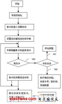
Figure 4 System software flow chart
Reader power consumption test results
When actually testing the designed system, it is often found that the power consumption is not as small as theoretically calculated. At this time, we must first distinguish whether the power is mainly consumed by the MCU itself or the peripheral circuit consumed by the I / O pin drive. The simplest way to judge is to measure the current of the MCU power input pin and the current of the MCU ground pin separately. Only when the values ​​of the two are basically equal, the power consumption of the entire system is the lowest. Can be analyzed from the following aspects: All input pins can not be left floating. If left floating, the digital input buffer will generate switching current, thereby increasing power consumption. All unused pins are set as outputs and set to a fixed high or low level. If the current of the MCU power input pin and the outflow current of the ground pin are not equal, the I / O pin must output or absorb the current, you should carefully find the output or absorb the current I / O pin and take measures to reduce power consumption . Check whether all on-chip peripheral circuits are turned off, otherwise the peripheral circuits will consume extra current.
The test results of this design are as follows: the standby current is 7mA, and the current is 38mA when reading and writing the IC card. The power consumption of the reader is closely related to the input voltage. As the input voltage increases, the power consumption of the reader also increases accordingly, so it is important to use the input voltage for reasonable options. If it is powered by 3 nickel-metal hydride batteries, the reader can work continuously for more than half a year. The design and implementation of the reader is tested, and the results show that: in general environment, the IC card can be found within the range of 0-8cm; the reading and writing distance is 0-4cm, and the various design functions of the work are completed normally, and the operation is stable. Technical index requirements.
However, this design needs to be improved in many aspects, for example, LCD display can be added to the reader, and a keyboard is added; this design does not take into account the software design of the host computer; the application can be further optimized to improve the program effectiveness.
USB C HUB,6 in 1 Type C Hub with Ethernet, 6 in 1 USB-C hub to HDMI,USB-C 6-in-1 Multiport Adapter,6 in 1 Multiport USB-C,USB-C Adapter Docking Hub
Shenzhen Konchang Electronic Technology Co.,Ltd , https://www.konchang.com