The most common purpose of computer-aided design technology (TCAD) applied to the design field is prediction, which enables engineers to understand the design. In some cases, simulations can be used to deal with something that cannot be measured in the lab. Simulations are increasingly used to increase manufacturing yields. When predictions are reliable, predictions have great advantages in the process of technology development. Although the predicted trend and quantity may sometimes differ from the measured actual data, in the vast majority of cases, TCAD can still provide the most accurate prediction based on available data.
Problems in the radio frequency (RF) field can be divided into two categories: small signal and large signal. The prediction of small signals based on TCAD is often difficult because copying the device characteristics into the simulator can be very complicated. In large-signal predictions, distortion may result due to operational limitations and imperfections in the device. In those instances where we can accurately simulate small-signal solutions, it is also possible to emulate large-signal solutions.
TCAD principleLet's take a look at the practical problem shown in Figure 1 where both small-signal and large-signal amplifiers have such problems. In the case of small signals, the amplifier is usually a class A amplifier. We assume that it is a conjugate match and the design is formulated. In the large-signal case, the amplifier can be AB or even B. The matching of the best performance in this case is usually not a conjugate match. The design of this large-signal amplifier is usually implemented in test laboratories by optimizing input and output matching networks, input bias and harmonic termination (harmonic terminaTIon). If these parameters and the intrinsic device design parameters are taken into account at the same time, a larger research space will be obtained. For multi-stage amplifiers that often use different technologies, it is possible that this parameter will increase dramatically.
To understand the performance of different device designs, we should not compare all device designs at the same matching, harmonic termination, and bias, but rather must compare those values ​​that yield the best performance of the device design. By comparing the optimal performance conditions of each device in the amplifier, the best performance device design choices can be made.
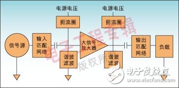
Figure 1: RF amplifier circuit.
This presents a clear case for all large-signal simulations of the circuit and device under consideration. If an engineer wants to evaluate new devices that do not have measured data at the time, they must use TCAD solutions. TCAD simulation of large-signal data is completed by four methods:
1. Adopt hybrid mode transient simulation in TCAD;
2. Use integrated harmonic balance (Harmonic Balance) for large-signal simulation directly in the TCAD tool;
3. Special tools integrate the composite simulation results with the circuit design;
4. Extract large signal compact models from TCAD data and use these models to understand large signal feature parameters.
It is very important to study the most basic method, that is, the possibility of simulation in mixed mode. In mixed mode, transient circuit simulations are done directly in the TCAD software. Under normal circumstances, circuit designers do not use transient simulations but use harmonic balance to solve these large-signal simulation problems. The challenge is to accurately describe the RF circuit within the workbench and then perform a TCAD simulation using a simple single (or dual) frequency carrier (CW) input power sweep. Transient simulation must be performed in steady state and may take several cycles. When the device is in compression, this simulation may face more numerical challenges. The simulated time series must be long enough to describe the required minimum frequency. For a two-tone or multiple tone problem, a long time transient simulation may be required. Therefore, running a power scan can be very time consuming. In addition, the design of the mixed-mode workbench is often very poor because it lacks key items such as complex resistance. For real circuits, the main problems with this approach are speed and convergence.
The second method is to achieve harmonic balance in the TCAD simulation tool. Harmonic balance method is more correctly called KCL-HB or Kirchhoff's current law harmonic balance for Agilent's Advanced Design System (ADS), Cadence's Spectre-RF, and commonly used in RF and analog designs. Other circuit simulators. Harmonic balance is a non-linear frequency domain technique used to determine quasi-periodic steady-state solutions for systems with wide frequency variations. This method uses the following equation:

The equation describes the relationship between linear and nonlinear circuit currents. The parameters in parentheses are linear and the rest are nonlinear. Is is the supply current, Y is the admittance matrix of the linear circuit, V is the internal node voltage vector, Ω is the angular frequency matrix on the diagonal, Q is the charge vector in the frequency domain, IG is in the frequency domain Nonlinear circuit current. When linear and nonlinear circuits reach equilibrium, this solution starts to converge.
Using TCAD's implementation requires a lot of development work. Although a large amount of research and university-originating procedures are available in this area, the market has not provided reliable tools. Harmonic balance is a method used for large-signal RF problems and is usually implemented in circuit simulation tools. Harmonic balance is a nonlinear frequency domain steady state simulation.
Linear circuit components are only modeled in the frequency domain, nonlinear components are modeled in the time domain, and are converted to the frequency domain at each step. The algorithm generally limits the number of harmonics of this process to 7 to 11 times. The memory requirement for 11 times is 4~8GB, not including the memory needed for device emulation. You can use iterative solutions that require less memory. Due to limited resources, these content requirements have led to the limitation of the number of harmonics, and analysis of multi-stage amplifiers cannot currently use this method. The scan may take several hours, and the actual device may take longer.
The third method was studied by Loechelt in 2000. This method calculates the load lift (CLP). In this method, simulations (or measurements) of large signal transients can be used to describe intrinsic devices, and tools are used to gather all of them together for circuit evaluation. This method has several advantages. Once a data set is created to describe the intrinsic device, it can be used in multiple circuit simulations. Of course, this method also has its disadvantages. Since the RF workbench is built inside the CLP tool, it can only be used for those designs that are executed in this tool.
So far, the problems with these methods are speed, RF workbench functionality, performance, and setup time, as described in Table 1.
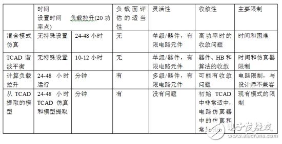
Table 1: Comparison of four methods for large-signal simulation of TCAD data.
The fourth method is to extract a compact model from TCAD simulation data. The main advantage of this method is that the simulation-based model uses the same program, extraction method, and can use the same design as the measurement-based model. This allows the use of very powerful RF circuit simulation functions and original RF designs that have been developed. The disadvantage is that it takes time to run TCAD, it takes time to extract the model, and the compact model used has some limitations. This is an important limitation because the physical features that TCAD simulation may contain cannot be reflected in compact models. There are two remedies for this kind of defect. One is to create a user-defined model version with better physical properties, and the other is to use a table-based model. In order to make this method practical, it is necessary to create an automatic extraction that enables rapid extraction of a large number of device models.
Since we know from Figure 1 that the best performance occurs in uncertain source and load matching, simulation must be performed at the entire source and load level to find the highest performance point. Assuming that 60 source states and 60 load states must be searched alternately, it is possible to complete about 300 power scans to determine the highest performance point.
Large Signal TCAD Simulation ExampleTCAD emulation is for devices using Synopsys tools. The model was extracted using methods that were automatically extracted from those already simulated, and the forward and reverse Gummel, I/Vs, and CV features shown in Figure 2 were compared.
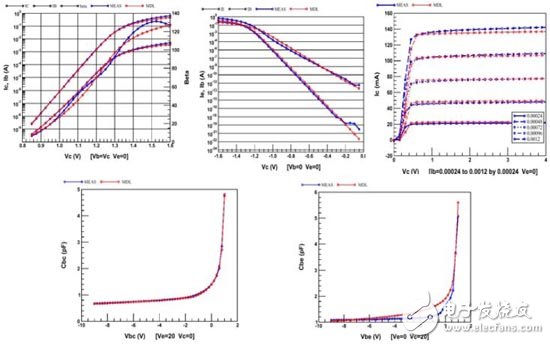
Figure 2: Comparison of forward and reverse Gummel, I/V, and CV features where TCAD data is blue and model data is red.
The TCAD data is displayed in blue and the model data is displayed in red. The two matches show that the model accurately reflects the original TCAD data. Figure 3 shows a comparison of S feature parameters. A good match again shows that the model accurately reflects the TCAD data.
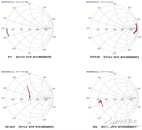
Figure 3: Comparison of S-parameter features, where TCAD data is blue and model data is red.
This model is used in a circuit similar to that shown in FIG. Use an algorithm that repeatedly scans the source and load planes to select the source and load match for the best performance. Fig. 4 compares the load plane efficiency between the data measured by similar design devices resulting from this, the black line is the reference measurement data, and the red line is the simulation data using this model.
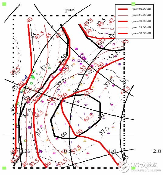
Figure 4: Efficiency contours.
The comparison of the power scan at the maximum efficiency point with the measured data of a similarly designed test device is shown in FIG. 5 .
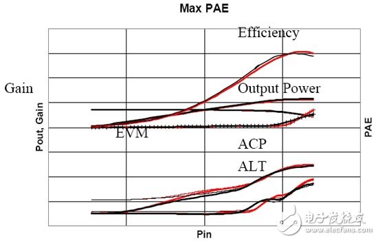
Figure 5: The highest efficiency power sweep.
This power scan shows excellent predictions of efficiency, output power, and gain. In addition, the comparison also shows the measurement results of linear error vector magnitude (EVM), adjacent channel power (ACP), and interphase channel power (ALT). These measurements show that the gain and phase relationships are well simulated. For current wireless communication device design, accurate prediction of linear characteristics, EVM, ACP, and ALT is very important.
Fan commonly refers to a Solar DC Fan a mechanical fan fitted with a DC motor and solar panels that charge up the fan through solar energy:
- Fan (machine), a machine for producing airflow, often used for cooling.
- Hand fan, an implement held and waved by hand to move air.
Benefits
1.Inverter-friendly: compatible with existing inverter solutions
2.Extracool wind3.AC/DC Solar Compatible
4.600% Energy-saving
5.High money saving on Electric bills
Dc Ceiling Fan,12V Dc Fan,Dc Brushless Fan,Dc Table Fan
NANTONG RONGCHANG IMPORT&EXPORT CO.,LTD , https://www.ergsolarcn.com