Step motor is an open-loop control element that converts an electrical pulse signal into an angular displacement e (or line displacement S) and is an actuator of a digital control system. The working principle is that the excited stator electromagnet attracts the optional rotating armature to generate torque and rotate, that is, the electromagnetic energy is converted into mechanical angular displacement by the magnet attraction. In the case of non-overloading, the speed and stop position of the motor depend only on the frequency of the pulse signal and the number of pulses, and are not affected by the load change, that is, a pulse signal is applied to the motor, and the motor rotates through a step angle. The number of pulses determines the size of the corner, and the frequency of the pulse determines the speed of the motor. The existence of this linear relationship, coupled with the stepper motor only periodic error without cumulative error. It is very simple to control the change with a stepping motor in the control field such as speed and position. General stepper motors can be divided into two phases, three phases, four phases and six phases.
The stepping motor of this system uses the VID29 series two-phase automobile instrument stepping motor of Shenzhen Weili Drive Co., Ltd. vID29-XX/VID29~xXp instrument stepper motor is a kind of precision stepping motor with built-in gear ratio of reduction ratio 180/1. It is mainly used in the instrument indicator plate of vehicles, and can also be used in other instrumentation devices. The digital signal is directly and accurately converted to the analog display output. The VID29 stepper motor requires two logic pulse signals to drive, and its characteristics are as follows:
Can work under 3.5V to 10V pulse;
The output shaft has a minimum step angle of 1/12 0 , a maximum angular velocity of 600 0 /s, and an output angle rotation range of 315 0 . It can be driven in step mode or micro step mode.
Imported high-quality special materials and automotive-grade special engineering plastics, while taking into account safety features such as fire protection;
This article refers to the address: http://
The special tooth profile with the lowest noise and ultra-low friction effect guarantees the long-term operating life and performance of the motor.
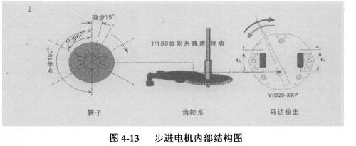
Step-by-step drive control mode of stepper motor: VID29 stepper motor is outputted by three-stage gear reduction. The drive requirement is to use standard SV logic circuit voltage. It can drive the motor directly in step-by-step drive mode with a current demand of 20mA. In the step mode, each pulse can drive the motor rotor to rotate 600 (ie, the output shaft rotates 1/3 degree). The direction in which the motor rotates depends on the phase difference of the periodic pulse sequence applied to the left and right coils of the motor. As shown in the figure below, when the left coil voltage UL phase leads the right coil voltage UR (phase difference is /3), the motor output shaft of the VID29-XX series will rotate clockwise, and the motor output shaft of the VID29-XXP series will rotate counterclockwise. .
The step-by-step driving mode pulse sequence is shown in Figure 4-14: 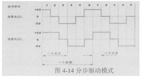
The micro-step drive mode (sub-driver) pulse sequence is shown in Figure 4-15:
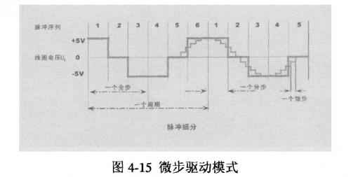
Its rotational speed n (or linear velocity v) is proportional to the pulse frequency f. The smaller the step angle, the smaller the angle of rotation of the pointer, and the higher the accuracy of the meter display. The relationship between the step angle and the pulse frequency can be calculated by the following relationship:
Φ=180*f/(I*S)
Where φ: step angle of stepper motor
f: pulse frequency
I: motor gear reduction ratio
S: drive mode distribution number (step/microstep)
The position and speed of the stepping motor are in a one-to-one correspondence between the number of times of conduction (number of pulses) and the frequency, and the direction is determined by the order of conduction.
Since the H128 integrates six stepper motor drive modules, the connection between the stepper motor and the H128 hardware interface circuit can be realized without extending the circuit. Through the distributed drive mode, each pulse can drive the stepper motor to rotate 1/3 degree, which meets the accuracy requirements of automotive instruments. (If higher precision is required, the stepper motor can be driven by each step by one step. 2 degrees). The hardware connection of the stepper motor and H128 is shown in Figure 4-16: 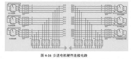
In the figure, PUO-PU7, PVO-PV7, PWO-PW7 are directly connected to the output pin of H128. Since each stepping motor is directly driven by H128, the stepping motor arrangement can be changed by modifying the program data output interface method.
4.8 Reset Circuit and E 2 PROM Design The MCU system is usually designed to perform or implement a certain function in a specific objective environment. Therefore, when the system is in working state, it is bound to be affected by various external interference factors. Such external interference factors may cause errors in the internal data of the system, and may even seriously affect the operation of the program, causing the microcontroller to be out of control and causing the program to run away or fall into an infinite loop. By taking certain hardware and software measures to get the program out of the infinite loop or re-run .
The system adopts the hardware method realized by the external expansion chip, and selects x5045[sll of xlc0R company. Integrated watchdog timer, EZPROM data memory, and power monitoring as one, connected to the MCU by SPI, used for low voltage reset signal microcontroller (H128 is low voltage reset). Because of its small size and small UO port, it has been widely used in industrial control, instrumentation and other fields.
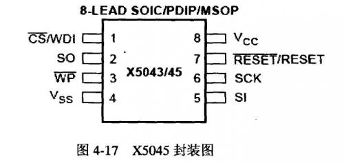
CS: chip select input, the chip is working when CS is low
50: Serial data output, on the falling edge of the serial clock, the data is output through the 50-side shift
Sl: serial data input, data is latched on the rising edge of the serial clock
SCK: Serial clock, providing serial bus timing for data read/write
WP: Write protection input. When WP is low, the write operation to X5045 is disabled, but other functions of the device are normal.
RESET: Reset signal output.
In addition to the wTD (watchdog) function, another important basic function of the x5045 is to use it as the EZPROM data memory. The internal 512xs serial EZPROM is used to ensure that the system can maintain important data after power failure. The x5045 and H128 use the SPI bus interface connection method to obtain an accurate pulse count and send this value to the X5045 storage. The X5045 is an ideal automatic storage non-volatile SRAM with an internal EEPROM and a storage capacity of 256 bits. It can automatically perform a storage operation (SRAM-EEPRoM) when the vCc is lost, which is very suitable for the cumulative recording of mileage. The chip contains an instruction shift register that can be accessed via the SPI. The circuit connecting X5045 and H128 is shown in Figure 4-18:
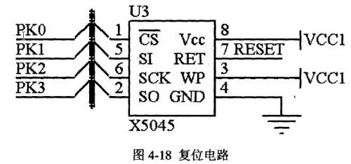
Among them, PKO-PK3 and RESET are respectively connected with corresponding pins on H128.
4.9 Other peripheral device circuit design
4.9.1 Crystal Oscillator Circuit
The crystal oscillator used in this system is SMHZ, which is corresponding to the pins XTAL and EXTAL of the H128 microcontroller, and then uses its internal voltage-controlled oscillator and phase-locked loop (PLL) to increase this frequency to 25MHZ, which acts as the internal bus for the microcontroller. clock. 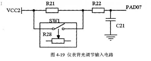
4.9.2 Instrument backlight adjustment circuit
The backlight of the instrument is always on after the car is started. The driver can adjust the backlight of the car according to the brightness of the external light in each environment to achieve the most suitable sensory effect. The instrument backlight circuit changes the resistance value by adjusting the potentiometer, thereby changing the magnitude of the current. The MCU changes the output of the PWM pulse width duty cycle according to the value of the received signal, thereby changing the brightness of the backlight 1401. The adjustment circuit diagram is as shown in FIG. 19: 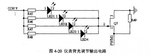
The switch SWI is an adjustable resistor, and the current is controlled by changing the size of the resistor, and is output to the A/D conversion interface RAD07 of the H128. The MCU adjusts the output duty ratio of the PWMI according to the data after the weekly D conversion, and the simulation obtained by the output interface CONV The quantity is related to the duty ratio. If the duty ratio is 1:1, the obtained voltage value is 1/2 of Vmax, that is, 2.5v. The change of the duty ratio causes the output voltage to change, thereby making the brightness of the instrument backlight display. Change 131]. Output backlight adjustment circuit as shown in Figure 4-20: 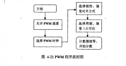
The program flow chart is relatively simple, and is directly analyzed here, as shown in Figure 4-21:
4.9.3 Status indicator circuit in the circuit of the car instrument
In the design, generally, according to the arrangement of peripheral electronic components, a combination of positive control (switch control positive circuit) and negative control (switch control negative circuit) is used to control various status indicators, and this design is also adopted in the instrument. method. The function indicator light adopts the bright LED, while the instrument illumination uses the high-brightness LED, which is divided into red, yellow and green colors, corresponding to different display and warning information. For LEDs and their corresponding current-limiting resistors, we use components in a chip package.
At the same time, after the engine fails, if the engine water temperature is too high, the corresponding fault light controlled by the MCU will flash. The engine has failed and its indication is generally red and accompanied by a buzzer alarm.
4.9.4 Voice Alarm Circuit
The instrument system has a buzzer alarm module, mainly to remind the driver to pay attention to relevant hazard information, such as: high water temperature, low water level, low oil pressure, gearbox failure and so on. The MCU compares the sampled data with the allowable value range stored in the EZPRoM unit. If the rated range is exceeded, the message is sent to the output port, the buzzer alarms, and the corresponding alarm indicator flashes. During the next sampling process, if the collected data is within the rated range, the buzzer will cancel the alarm and the status indicator will go out.
The buzzer selected in this system is frequently short and tweet, the frequency is 2.6KHz, and the volume is 75db. Since the system UO port resources are very rich, one port can be shared, and one port can be occupied separately, which occupies the port separately, which is beneficial to fault repair. Check, the system reserves BPO-BP3 as the alarm circuit output port on H128.
4.9.5 Clock Generator
The circuit RTC module (real-time clock circuit) has a memory-mapped register, the time provided by the seconds, minutes, and hour counters; the calendar function is provided by day, day, month, and year. Each of the above counters can generate an interrupt each time it is incremented, and the corresponding interrupt flag is set separately. If the corresponding interrupt is enabled, a CPU interrupt request can be generated.
The IHZ clock used to drive time and calendar allows the embedded compensation unit to compensate for crystal error, which allows the IHZ clock to achieve higher accuracy for the crystal used to drive the entire module.
The compensation value can be set or automatically acquired by the application software during the calibration operation of the module.] The timing function is realized by a counter with a clock frequency of 128 Hz (CGMXCLK/256).
This counter can be started at any time. Stop and clear. The value of this counter is converted to the value corresponding to looHZ and stored in the timing data register (chronographdatarcgister). Therefore, the value in the data register is 0 to 99, and each additional 1 represents 1/1005 (loms). The value of the data register satisfies the following relationship: S = "(128HzeountervalueX25) + 16] / 32 The accuracy of the timing counter is sms.
4.10 PCB board design
In the past instrument circuit design process, the circuit of the instrument is usually attached with a layer of soft plastic (flexible plastic) on the back of the instrument, and copper is connected to the circuit for circuit connection. This connection is usually applied to a relatively simple circuit. Due to the development of electronic technology, soft plastics can not meet the requirements of a wide range of instrument functions, and gradually
Hard board replaced. That is, printed boards, commonly referred to as PcB boards.
The difference between board design and circuit diagram design is that the board is a relatively materialized thing, and the circuit diagram is a relatively abstract thing. Therefore, when designing the circuit diagram, the electrical properties of the circuit are emphasized. When designing a circuit board, the actual size and space configuration (stereo) of the circuit are emphasized. The following is the following steps on the design of the circuit board;
In the first step, the circuit diagram is first designed to determine the ordering of components and the packaging of the components (Footprint), and then through the ERC check provided by the program.
In the second step, after the circuit diagram design is completed, the network table is generated by using the CreateNetlist function.
The third step, enter the PCB editor, first define the board frame, that is, the size of the board, the number of layers and the shape.
The fourth step, loading the network table, if the network table (or circuit diagram) has errors, or problems on the interface, will appear in this phase. It can be modified to the circuit diagram according to the error generated.
The fifth step, the layout of components, this work is the most basic, most troublesome and most influential work in circuit board design.
The sixth step is to define the design rules for manual routing or automatic routing.
In the seventh step, after the wiring is completed, the design verification check is performed. If no errors are found, you can save the output.
Printed boards usually have paper clad laminates, epoxy boards, fiberglass boards, etc. Here, considering the price factor and performance requirements, we choose epoxy resin board, which is moderately priced and can also meet the work of car operation. Environment, PCB uses double-sided wiring, and adds pad measurement points in some signal circuits to facilitate the detection of instrument circuit functions and reduce the fault repair rate.
Dc Power Contactor,Contactor Relay,Dc Contactor Relay,Dc Magnetic Contactor
NanJing QUANNING electric Co.,Ltd , https://www.quanningtrading.com