With the arrival of the start of school in September, the anticipated and tense job hunt has also begun. As someone who has come, I certainly know the anxiety and anxiety in everyone's mind~~"What are the knowledge points of PCB?" "What is the job of a PCB designer?" "What kind of knowledge and skills do I have to stand out in the workplace? ...
STOP! Don't panic~ In fact, it's not just you who are looking for a job. Many new PCB newcomers who have just joined the job also lack a comprehensive and systematic understanding of PCB design. The so-called infrastructure determines the superstructure, and solid basic knowledge is the only way to advance in the future~
The editor specially invited Cadence senior expert, former Huawei PCB designer, and Ms. Fairy Zheng, who has more than 8 years of PCB design experience, to introduce newcomers to PCB introductory knowledge and share her experience and experience for many years in the industry, hoping to make novices avoid detours. Have an in-depth understanding of PCB design knowledge quickly and comprehensively.


Come and follow the editor to make notes and focus!
PCB Newcomer's Book · Basic Theory of Chapter One
This chapter will test everyone's mastery of the basic knowledge of PCB design through the way of answering questions in the test paper. The content of the topic includes knowledge of PCB concepts, categories and physical structure.
Start to answer the question:
1. Fill in the blanks: The abbreviation of PCB is (), the full name is ()
Answer: The abbreviation of PCB is (Printed Circuit Board), the full name is (Printed Circuit Board)
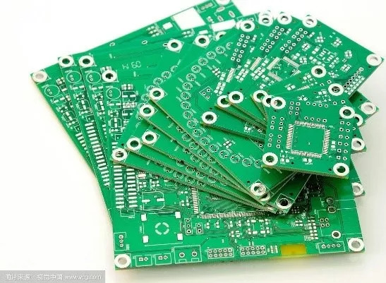
Note: PCB-the abbreviation of Printed Circuit Board, that is, printed circuit board, is to realize the connection relationship shown in the circuit diagram through certain technological capabilities and realize it on a certain special material. It is an actual functional module. As shown in the example.

2. Fill in the blank questions: PCB is divided by the number of layers, which can be divided into (), () and ()
Answer: PCB is divided according to the number of layers, which can be divided into (single-sided board), (double-sided board) and (multi-layer board)
Note: The single-sided board means that the devices are concentrated on one side of the PCB, and the wires are concentrated on the other side. Since the wires only appear on one side, it is called a single-sided; a double-sided board is an extension of a single-sided board. When a single-layer wiring cannot meet the needs of electronic products, a double-sided board should be used. There are traces on both sides of the double-sided board, and the lines between the two layers are connected through via holes; the multilayer board refers to the conductive pattern layer with more than three layers, and the patterns of each layer can also be connected through via holes as required. Multilayer board is the product of PCB development towards high speed, high density and direction.
3. Questions and answers: According to characteristics, PCB can be divided into flexible board (FPC), rigid board (PCB), rigid-flex board (FPCB). Please explain the concept and purpose of flexible board and rigid-flex board respectively.
Answer: Flexible Printed Circuit Board (Flexible Printed Circuit Board) is a printed circuit made of a flexible insulating substrate, which can be freely bent, wound, and folded, and arranged arbitrarily according to the space layout requirements. Rigid-flex board refers to a PCB that contains one or more rigid areas and flexible areas, which is composed of a rigid board and a flexible board laminated together, which can meet the needs of three-dimensional assembly.
4. True or False: Is the physical shape of the finished PCB necessarily regular?
Answer: Wrong. Many PCBs have irregularities and irregularities.

The picture comes from the internet: a more regular PCB processed
5. Questions and answers: Briefly describe the position and function of solder mask oil.
Answer: The solder mask is on the outermost layer of the PCB. The solder mask is applied to the surface of the PCB to protect the circuit on the board from being short-circuited by foreign objects and to cover the copper wire on it, so that the copper wire is not easy to fall off.
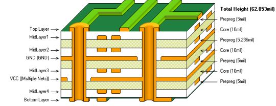
Note: The solder mask in the picture above is green. Nowadays, there are not only green solder masks on the market, but also other colors such as red and black.
Supplementary knowledge points: As can be seen from the above cross-sectional view, the PCB is laminated by core+PP, and the different conductive layers are connected through vias.
This is the end of the test paper answering questions, how did everyone perform~
After finishing the basic knowledge, Mr. Fairy will explain the PCB design process for everyone in the next chapter. Please prepare your notebook~
The utility model relates to a medical atomization treatment and humidifying device belonging to the technical field of medical equipment and household appliances.
Professional Medical Atomization manufacturer is located in China, including Medical Vape,Dose Control Vape Pen,Supersonic Wave Vape, etc.
Medical Atomization,Medical Vape,Dose Control Vape Pen,Supersonic Wave Vape
Shenzhen MASON VAP Technology Co., Ltd. , https://www.e-cigarettefactory.com