[Audio Network Information] Real-world signals such as vibration, temperature, pressure, and light require precise signal conditioning and signal conversion before further data processing can be performed in the digital domain. To overcome the many challenges of today's high-precision applications, a well-designed low-noise analog front end is required to achieve the best signal-to-noise ratio (SNR). Many systems can't afford the most expensive devices, nor can they withstand the higher power consumption of low-noise devices. This paper presents a systematic approach to design a gain block and ADC combination and gives an example of supporting this method. The circuit performs noise calculations and analysis while conditioning low frequency (close to dc) signals.
When designing the analog front end, follow these seven steps: 1) describe the electrical output at the front of the sensor or gain block; 2) calculate the ADC's requirements; 3) find the best ADC + reference voltage for signal conversion; 4) for the op amp Find the maximum gain and define the search conditions; 5) find the best amplifier and design the gain module; 6) check the solution total noise according to the design goals; 7) run the simulation and verify.
Step 1: Describe the electrical output at the front of the sensor or gain block. The signal may come directly from the sensor or through the EMI and RFI filters before reaching the gain block. In order to design the gain block, the ac and dc characteristics of the signal and the available power supply must be known. Knowing the characteristics of the signal and the noise level, we know what input voltage range and noise level are needed to select the ADC. Suppose there is a sensor that outputs a 10 kHz signal at full scale amplitude of 250 mV pp (88.2 mV rms) and 25 μV pp noise. We further assume that there is a 5V power supply available in the system. With this information, we should be able to calculate the signal-to-noise ratio at the ADC input in step 2. To simplify data processing and avoid confusion, let's assume that the solution is designed to work at room temperature.
Step 2: Calculate the ADC's needs <br> What kind of ADC do we need, what is the sampling rate, how many bits, and what are the noise specifications? If we know the input signal amplitude and noise information from the first step, we can calculate the signal-to-noise ratio (SNR) at the input of the gain block. We need to choose an ADC with a better signal to noise ratio. Knowing the SNR will help us calculate the effective number of bits (ENOB) when choosing an ADC.
The ideal ADC data sheet always marks SNR and ENOB. The 86.8 dB SNR and 14.2 ENOB required in this example determine that we should choose a 16-bit analog-to-digital converter. In addition, the Nyquist criterion requires that the sampling rate (fs) be at least twice the maximum input frequency (fin), so a 20-kSPS ADC should be sufficient. Next we need to design the overall solution so that the noise density does not exceed 416 nV/rt-Hz.
Step 3: Find the best ADC + reference voltage for signal conversion <br> With a range of search conditions, we have many ways to find the right ADC. One of the easiest ways to find a 16-bit ADC is to use the search tool on the manufacturer's website. Enter the resolution and sample rate to find many recommended ADCs.
Many 16-bit ADCs meet the 14.5-bit ENOB requirement. If you want better noise performance, you can use oversampling to force ENOB up to 16 bits (next enhancement by 4^n oversampling). With oversampling, you can use a lower resolution ADC: a 256 oversampled 12-bit ADC (4^4 oversampling) for 16-bit noise performance. In our case, this means a 12.12 MHz sample rate 12-bit ADC (20 kSPS × 256) or a 4^2 oversampled 14-bit ADC; if 1.28 MSPS is better. However, the cost of these options is comparable to the AD7685 (16-bit, 250 kSPS ADC).
The AD7685 reference input has a dynamic input impedance and therefore needs to be decoupled to minimize parasitic inductance by placing a ceramic decoupling capacitor near the pin and connecting it with a wide low impedance trace. A 22 μF ceramic chip capacitor provides the best performance.
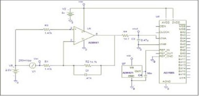
Step 4: Find the maximum gain for the op amp and define the search conditions. <br> Having the input voltage range of the ADC will help us design the gain block. To maximize dynamic range, we need to choose the highest possible gain for a given input signal and ADC input range. This means that we can design the gain block in this example to have a gain of 10 times.
Although the AD7685 is easy to drive, the driver amplifier needs to meet certain requirements. For example, to maintain the SNR and conversion noise performance of the AD7685, the noise generated by the driver amplifier must be as low as possible, but be aware that the gain block can amplify both the signal and the noise. To keep the noise constant before and after the gain block, we need to select the amplifier and associated components with lower noise values. In addition, the driver's THD performance should be comparable to that of the AD7685, and the ADC capacitor array must be built to a full-scale step at 16-bit levels (0.0015%). The noise from the amplifier can be further filtered using an external filter.
How much noise does the input of the op amp allow? Keep in mind that the overall solution we designed does not exceed 416 nV/rt-Hz. The gain block we designed should have a lower noise floor with a factor of 10 because our gain is 10. This will ensure that the noise from the amplifier is much lower than the noise floor of the sensor. When calculating the noise margin, we can assume that the noise at the input of the op amp is roughly equal to the total noise of the op amp plus the noise of the ADC.
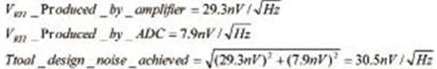
Step 5: Find the best amplifier and design the gain block <br> After knowing the input signal bandwidth, the first step in op amp selection is to choose an operational amplifier (GBWP) with a reasonable gain-bandwidth product (GBWP), and The amplifier processes the signal with minimal DC and AC errors. To get the best gain-bandwidth product, you need to know the signal bandwidth, noise gain, and gain error. The definitions of these terms are given below. In general, if you want to keep the gain error less than 0.1%, it is recommended to use an amplifier with a gain bandwidth that is 100 times larger than the input signal bandwidth. In addition, we need an amplifier that can be quickly built and has good drive capability. Note that our noise budget requires that the total noise at the op amp input is below 40.8 nV/rt-Hz, while the ADC specifies a 7.9-nV/rt-Hz. Summary The operational amplifiers are searched for the following conditions: UGBW>1MHz, 5-V single supply, good voltage noise, current noise, THD characteristics, low DC error (does not degrade ADC performance).
A similar search method was used to search for the ADC. In this case, we selected the AD8641. The AD8641 is a low power, precision JFET input amplifier with very low input bias current and rail-to-rail output capability that operates from a 5 V to 26 V supply. The relevant data is listed in the table below. We can use the component values ​​in the table to configure the op amp in phase.
All active and passive components each generate noise, so it is especially important to choose components that do not degrade performance. For example, buying a low-noise operational amplifier and placing a large resistor around it is a waste. Keep in mind that a 1 kohm resistor can generate 4 nV of noise.
Complete solution
Step 6: Check the total noise of the solution according to the design goals <br> It is extremely important to fully understand the various sources of error in the designed circuit. In order to get the best SNR, we need to write the total noise equation of the previous scheme.

Equation 1
We can calculate the total noise at the input of the op amp and make sure it is below 41.6 nV/rtHz, as we expected.
Equation 2
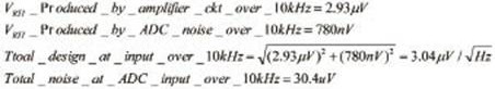
To integrate the total noise over the entire bandwidth, we can see that the total noise at the ADC input on the filter bandwidth is 3.05μV, which is lower than the 4.16μV required for the design. Since the corner frequency of the AD8641 is lower than 100 Hz, the low frequency noise (1/f) in this example is negligible.
Equation 3
Maintaining a good signal-to-noise ratio requires attention to the noise of every detail in the signal path and a good PCB layout. Avoid placing digital lines underneath any ADC, otherwise noise will be coupled to the chip die unless a ground plane is placed under the ADC for shielding. Fast switching signals such as CNV or clocks should not be close to the analog signal path. Avoid overlapping digital signals with analog signals.
Step 7: Run the simulation and verify <br> When you first verify the circuit design, it is appropriate to use the Pspice macro model (available from the ADI website). The fast simulation shows the signal bandwidth we have designed for the solution. Figure 5 shows the response before and after the optional RC filter at the input of the AD7685.
As shown in Figure 6, the total output noise on the 10-kHz bandwidth is close to 31μV rms, which is slightly lower than the design goal of 41μV rms. Prototypes and verification of the entire solution are required before mass production.
![]()
Noise response simulation of the circuit shown in Figure 6.
Summary: Many designs today require low power and low cost, and many systems can't afford the most expensive devices or the higher power consumption of low noise devices. In order to get the lowest noise floor and best performance from the signal conditioning circuit, designers must understand the noise level at the component level. Maintaining a good signal-to-noise ratio requires attention to the noise of every detail of the signal path. By following the steps above, you can successfully condition small analog signals and convert them using an ultra-high resolution ADC.
When designing the analog front end, follow these seven steps: 1) describe the electrical output at the front of the sensor or gain block; 2) calculate the ADC's requirements; 3) find the best ADC + reference voltage for signal conversion; 4) for the op amp Find the maximum gain and define the search conditions; 5) find the best amplifier and design the gain module; 6) check the solution total noise according to the design goals; 7) run the simulation and verify.
Step 1: Describe the electrical output at the front of the sensor or gain block. The signal may come directly from the sensor or through the EMI and RFI filters before reaching the gain block. In order to design the gain block, the ac and dc characteristics of the signal and the available power supply must be known. Knowing the characteristics of the signal and the noise level, we know what input voltage range and noise level are needed to select the ADC. Suppose there is a sensor that outputs a 10 kHz signal at full scale amplitude of 250 mV pp (88.2 mV rms) and 25 μV pp noise. We further assume that there is a 5V power supply available in the system. With this information, we should be able to calculate the signal-to-noise ratio at the ADC input in step 2. To simplify data processing and avoid confusion, let's assume that the solution is designed to work at room temperature.
Step 2: Calculate the ADC's needs <br> What kind of ADC do we need, what is the sampling rate, how many bits, and what are the noise specifications? If we know the input signal amplitude and noise information from the first step, we can calculate the signal-to-noise ratio (SNR) at the input of the gain block. We need to choose an ADC with a better signal to noise ratio. Knowing the SNR will help us calculate the effective number of bits (ENOB) when choosing an ADC.
The ideal ADC data sheet always marks SNR and ENOB. The 86.8 dB SNR and 14.2 ENOB required in this example determine that we should choose a 16-bit analog-to-digital converter. In addition, the Nyquist criterion requires that the sampling rate (fs) be at least twice the maximum input frequency (fin), so a 20-kSPS ADC should be sufficient. Next we need to design the overall solution so that the noise density does not exceed 416 nV/rt-Hz.
Step 3: Find the best ADC + reference voltage for signal conversion <br> With a range of search conditions, we have many ways to find the right ADC. One of the easiest ways to find a 16-bit ADC is to use the search tool on the manufacturer's website. Enter the resolution and sample rate to find many recommended ADCs.
Many 16-bit ADCs meet the 14.5-bit ENOB requirement. If you want better noise performance, you can use oversampling to force ENOB up to 16 bits (next enhancement by 4^n oversampling). With oversampling, you can use a lower resolution ADC: a 256 oversampled 12-bit ADC (4^4 oversampling) for 16-bit noise performance. In our case, this means a 12.12 MHz sample rate 12-bit ADC (20 kSPS × 256) or a 4^2 oversampled 14-bit ADC; if 1.28 MSPS is better. However, the cost of these options is comparable to the AD7685 (16-bit, 250 kSPS ADC).
The AD7685 reference input has a dynamic input impedance and therefore needs to be decoupled to minimize parasitic inductance by placing a ceramic decoupling capacitor near the pin and connecting it with a wide low impedance trace. A 22 μF ceramic chip capacitor provides the best performance.
Step 4: Find the maximum gain for the op amp and define the search conditions. <br> Having the input voltage range of the ADC will help us design the gain block. To maximize dynamic range, we need to choose the highest possible gain for a given input signal and ADC input range. This means that we can design the gain block in this example to have a gain of 10 times.
Although the AD7685 is easy to drive, the driver amplifier needs to meet certain requirements. For example, to maintain the SNR and conversion noise performance of the AD7685, the noise generated by the driver amplifier must be as low as possible, but be aware that the gain block can amplify both the signal and the noise. To keep the noise constant before and after the gain block, we need to select the amplifier and associated components with lower noise values. In addition, the driver's THD performance should be comparable to that of the AD7685, and the ADC capacitor array must be built to a full-scale step at 16-bit levels (0.0015%). The noise from the amplifier can be further filtered using an external filter.
How much noise does the input of the op amp allow? Keep in mind that the overall solution we designed does not exceed 416 nV/rt-Hz. The gain block we designed should have a lower noise floor with a factor of 10 because our gain is 10. This will ensure that the noise from the amplifier is much lower than the noise floor of the sensor. When calculating the noise margin, we can assume that the noise at the input of the op amp is roughly equal to the total noise of the op amp plus the noise of the ADC.
Step 5: Find the best amplifier and design the gain block <br> After knowing the input signal bandwidth, the first step in op amp selection is to choose an operational amplifier (GBWP) with a reasonable gain-bandwidth product (GBWP), and The amplifier processes the signal with minimal DC and AC errors. To get the best gain-bandwidth product, you need to know the signal bandwidth, noise gain, and gain error. The definitions of these terms are given below. In general, if you want to keep the gain error less than 0.1%, it is recommended to use an amplifier with a gain bandwidth that is 100 times larger than the input signal bandwidth. In addition, we need an amplifier that can be quickly built and has good drive capability. Note that our noise budget requires that the total noise at the op amp input is below 40.8 nV/rt-Hz, while the ADC specifies a 7.9-nV/rt-Hz. Summary The operational amplifiers are searched for the following conditions: UGBW>1MHz, 5-V single supply, good voltage noise, current noise, THD characteristics, low DC error (does not degrade ADC performance).
A similar search method was used to search for the ADC. In this case, we selected the AD8641. The AD8641 is a low power, precision JFET input amplifier with very low input bias current and rail-to-rail output capability that operates from a 5 V to 26 V supply. The relevant data is listed in the table below. We can use the component values ​​in the table to configure the op amp in phase.
All active and passive components each generate noise, so it is especially important to choose components that do not degrade performance. For example, buying a low-noise operational amplifier and placing a large resistor around it is a waste. Keep in mind that a 1 kohm resistor can generate 4 nV of noise.
Complete solution
Step 6: Check the total noise of the solution according to the design goals <br> It is extremely important to fully understand the various sources of error in the designed circuit. In order to get the best SNR, we need to write the total noise equation of the previous scheme.
Equation 1
We can calculate the total noise at the input of the op amp and make sure it is below 41.6 nV/rtHz, as we expected.
Equation 2
To integrate the total noise over the entire bandwidth, we can see that the total noise at the ADC input on the filter bandwidth is 3.05μV, which is lower than the 4.16μV required for the design. Since the corner frequency of the AD8641 is lower than 100 Hz, the low frequency noise (1/f) in this example is negligible.
Equation 3
Maintaining a good signal-to-noise ratio requires attention to the noise of every detail in the signal path and a good PCB layout. Avoid placing digital lines underneath any ADC, otherwise noise will be coupled to the chip die unless a ground plane is placed under the ADC for shielding. Fast switching signals such as CNV or clocks should not be close to the analog signal path. Avoid overlapping digital signals with analog signals.
Step 7: Run the simulation and verify <br> When you first verify the circuit design, it is appropriate to use the Pspice macro model (available from the ADI website). The fast simulation shows the signal bandwidth we have designed for the solution. Figure 5 shows the response before and after the optional RC filter at the input of the AD7685.
As shown in Figure 6, the total output noise on the 10-kHz bandwidth is close to 31μV rms, which is slightly lower than the design goal of 41μV rms. Prototypes and verification of the entire solution are required before mass production.
Noise response simulation of the circuit shown in Figure 6.
Summary: Many designs today require low power and low cost, and many systems can't afford the most expensive devices or the higher power consumption of low noise devices. In order to get the lowest noise floor and best performance from the signal conditioning circuit, designers must understand the noise level at the component level. Maintaining a good signal-to-noise ratio requires attention to the noise of every detail of the signal path. By following the steps above, you can successfully condition small analog signals and convert them using an ultra-high resolution ADC.
The design of the terminal blocks with clamping yoke connections which has contact pressure and has with self-locking function.Providing test type,knife Disconnect,fuse type terminal blocks etc.The cross-sectional is 0.5-35mm².
Marker Carrier For Terminal,Screw Connection End Stopper,Terminal Block End Stopper,Terminal Connection End Clip
Wonke Electric CO.,Ltd. , https://www.wkdq-electric.com