1 Introduction
With the large number of applications of communication equipment and computer network equipment, the power supply to such equipment requires 24 hours of continuous operation. In the past, the need to shut down the power module equipment was unacceptable for communication network equipment. At present, the requirements for output power in a large power system are various, sometimes requiring redundant backup or load with the equipment. Adding or removing power modules, adding or removing power modules must ensure that all devices work properly. Hot plugging technology is the way to solve such problems.
2 Problems that need to be solved to achieve hot plugging:
When a power module is inserted into a working power backplane, due to the input capacitance in the power supply circuit, a large charging transient current is generated when the input capacitor is charged. This will cause glitches (which may affect other boards) and may cause permanent damage to the power supply. The key to allowing hot plugging is to control the power supply input. Usually, the operating current of the control FET is slowly changed from small to large until the input capacitor is full of charge. When the input capacitor is fully charged, the FET is fully turned on and the circuit is powered directly from an external source.
3 Function introduction:
The ISL6140 is a negative voltage hot-swap type controller from INTERSIL. It allows the power module to be safely removed or plugged in from the working power backplane. The limit value of the inrush current can be realized by controlling the gate rising voltage of the external N-channel FET. If the input voltage is above or below the design input voltage range, the switch will turn off. A programmable electronic circuit breaker protects the entire system when the system is shorted. In addition, the IC also provides a signal output for direct display of the normality of the input supply voltage.
The ISL6140 uses few external components and has strong control functions. It is suitable for DC-DC pre-stage hot-swap and over-current, over-voltage and under-voltage protection.
IC features:
External power supply negative N-channel FET
Operating voltage range from -10V to -80V (-100V rated maximum) or from +10V to +80V (+100V rated maximum)
Inrush current value can be set by itself
Programmable electronic circuit breaker (overcurrent shutdown)
Programmable overvoltage protection
Programmable low voltage cutoff
Input voltage status display
Application areas:
VOIP (Voice Over Internet Protocol) server
-48V telecommunication system
Negative voltage supply control
+24V wireless base station power supply
IC pin and circuit internal structure introduction:
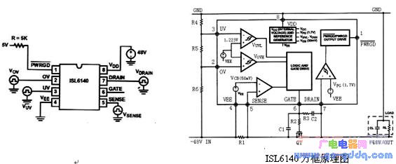
PIN1 PWRGD : Power status signal output
PIN2 OV (Over-Voltage) : Overvoltage protection detection terminal
PIN3 UV (Under-Voltage): Undervoltage protection test terminal
PIN4 VEE: Usually the negative side of the power supply
PIN5 SENSE : Overcurrent detection terminal, generally connected to a resistor
PIN6 GATE : Gate drive end of N-channel FET
PIN7 DRAIN : Drain terminal of N-channel FET
PIN8 VDD : voltage positive input
4 Peripheral component parameter calculation:
Calculation of 1VUVL and VOVH:
VUVL and VOVH are the allowable fluctuation ranges of the input voltage of the circuit. In this range, the N-channel FET of the IC control is turned on, and the circuit works normally. Once the input voltage exceeds this range, the N-channel FET is turned off. The IC defines VUVL and VOVH through two operational amplifiers. In addition, the three voltage dividing resistors R4, R5, and R6 should be selected with high precision and small temperature coefficient (for example, 1% metal oxide film resistor).
The calculation formula is as follows:
VUV=1.223(R4+R5+R6)/(R5+R6)
VOV=1.223(R4+R5+R6)/(R6)
The voltage waveform triggered by the circuit is shown below:
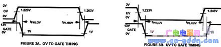
Tphlov: 0.6~3.0us Typical value: 1.6us Tplhov: 1.0~12.0us Typical value: 7.8us
Tphluv: 0.6~3.0us Typical value: 1.3us Tplhuv: 1.0~12.0us Typical value: 8.4us
2N channel FET selection:
N-channel FET is a key component of the circuit, and the parameters of the device should be considered from the following aspects:
Maximum input voltage (including transient shock) and output transient voltage; maximum operating current; FET dissipated power or safe working area; FET gate threshold voltage; FET on-state resistance (RDSOn ). The selected FET should consider sufficient margin and economy based on the above conditions.
3 current limiting resistor selection:
R1 is an overcurrent detection resistor. As long as more than 50mV is detected on R1, the voltage on the GATE pin will go low and the FET will turn off. Therefore, as long as the current value of the circuit overcurrent protection is set, the value of R1 can be calculated.
R1=V/Ioc=0.05V/Ioc
4R2, C1, R3, C2 parameter selection:
R2 can take a typical value of 10Ω
R3 and C2 are feedback networks for controlling the inrush current.
I inrush current = (I gate current *CL) / C2 CL - load capacitance; I gate current - N-channel FET gate charging current 45uA
C2=(45uA*CL)/I inrush current
C1=(Vinmax-Vth)/Vth*(C2+Cgd)
Vinmax - maximum input voltage; Vth - FET minimum gate threshold voltage; Cgd - FET drain capacitance
R3=(Vinmax+ΔVgate)/5mA Typical value is 18KΩ
5 power signal output design
PWRGD is a power signal output port that can intuitively display the input status of an external power supply.
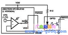
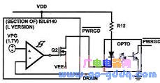
Optocoupler output mode LED display mode
The optocoupler output mode can be used to control the soft start function of the PWM control chip of the latter stage.
LED display mode shows the status of the input voltage very intuitively
If no external signal output is required, the port should be left floating.
5 Several issues to be aware of in actual circuit design:
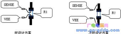
1R1 resistor selection points and wiring requirements
The PCB layout design of R1 has a great influence on the circuit. In the actual design process, the influence of external interference must be minimized. In addition, since R1 is in the main circuit of input and output, the width of the PCB trace should be wide enough during the circuit design process, not only to meet the needs of normal operating current but also to meet the requirements of high current during overcurrent protection. The ideal R1 wiring should be connected directly to the PIN4 (VEE) at the other end and directly connected to the PIN5 (SENSE). The position should be as close as possible and the length of the trace should be as short as possible. For example, the following figure:
2 method for suppressing transient overcurrent pulse
In order to make the instantaneous overcurrent in the circuit not turn off the power supply, a filter can be connected across R1.
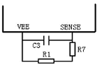
If the instantaneous current pulse width to be suppressed exceeds 3us (less than 3us is controlled by the built-in filter of the IC), a low-pass filter consisting of C3 and R7 as shown in the figure above is required to filter out. The value of R7 should not be too large. It is recommended to use 100Ω. The width of the pulse is determined by:
t= ─R*C*ln[1-(V(t)-V(t0))/(Vi-V(t0))]
V(t)----trigger voltage
Vi----voltage on R1 during overcurrent protection
V(t0)----the voltage of current on R1 during normal operation
For example, there is a normal operating current of the system is 1A, overcurrent protection at 2.5A, R1 is 20mΩ, and current pulses of 50us and 5A must be filtered out. Calculated as follows:
V(t)=50mV (system specification)
V(t0)=20mV (V=I*R=1A*20mΩ)
Vi=100mV (V=I*R=5A*20mΩ)
If R1=100Ω then C3 should be 1uF
Note: N-channel FETs should be selected for models that can continue to pass more current, because the IC can not limit the current, the RC filter only delays
Turn off the effect of the FET. If the operating current of the FET is less than the current value of the transient overcurrent, the FET may be damaged.
3OV and UV application notes
R4 is much larger than R5 and R6. When selecting the resistance parameter, R4 is selected first, and the sink current of OV and UV is set at about 100uA.
For example: 50V input voltage, R4 can choose 500KΩ, then R5, R6 can choose about 10KΩ resistor. In order to eliminate the influence of external transient pulses on the circuit, it is also a good method to add a filter between UV to VEE or OV and UV.
4IC overvoltage protection requirements
The ISL6140 itself can only withstand a maximum voltage rating of 100V. Even a brief overvoltage will cause permanent damage to the IC and affect other components. In order to protect the IC, a surge absorber can be added between the VDD and VEE of the IC (for example, DIODE's SMAT70A, absorption power 400W, maximum breakdown voltage 89V, minimum breakdown voltage 70V, reverse maximum pulse current 3.5A) . The selection of the surge absorber is based on the normal input voltage variation range of the power supply, the expected amount of power to be absorbed, and the maximum reverse pulse current.
6 Summary
With the wide application of DC-DC modules and the increasing demand for high-performance power supplies in communication network equipment, hot-swap control chips will be further applied with a small number of peripheral components, multiple protection functions, and good cost performance.
door opener keychain no touch,no touch keychain,no touch tool keychain,no touch keychain bulk, no touch keychain wholesale
Shenzhen Konchang Electronic Technology Co.,Ltd , https://www.konchangs.com