Chen Xinglong, Tang Hai, Ren Peng, Li Jian, The 29th Institute of China Electronics Technology Corporation
Keywords: I2C bus; FPGA; finite state machine; Verilog HDL
introduction
Currently, buses used in communications are serial buses and parallel buses. Compared with parallel buses, serial buses have low cost, occupy few pins, and have simple structure. In the project more commonly used serial bus I-wire, IEEE1394, USB and I2C, etc., which I2C bus has a simple and practical features, in serial EEPROM, microcontroller, digital potentiometer and other devices are widely used.
The I2C bus is an abbreviation of the English Inter IC BUS. It was first developed by Philips of the Netherlands. The I2C bus only requires two serial data lines for data transmission: the data line SDA and the clock line SCL, which can be used for bidirectional and binary data synchronous serial transmission. It allows several IC terminals to be connected on the bus. Each IC terminal has a separate address as an identification identifier, and each has a function of sending and receiving data, so that data information exchange between IC terminals connected to the bus can be realized.
Most of the I2C-bus interface chips that exist on the market today are dedicated chips. Although the price is relatively low, it is convenient to use them. However, the functional performance is single, the versatility is not strong, and the selectable address range is small. For FPGA system programmable, easy to debug, and online configuration features, programmable devices can be selected to implement the I2C bus design and application, which can enhance the versatility of the I2C bus function, and greatly reduce the system development cycle.
1 I2C bus data transmission protocol
To achieve normal data transmission, the I2C bus must comply with the data transmission timing requirements specified in the I2C bus data transmission protocol. I2C bus for a complete data transmission timing requirements shown in Figure 1.
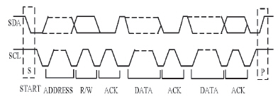
Figure 1 I2C bus complete data transmission sequence
The I2C bus uses the clock synchronization signal to realize the synchronous transmission of data. The signals related to the data transmission mainly include a start signal, an address signal, a read/write control signal, an answer signal, a data transmission signal, and a termination signal.
The I2C bus operation sequence is described as follows:
(1) When communication starts, on the master side, when the clock line (SCL) is high, the data line (SDA) transitions from high level to low level.
(2) The master sends 7-bit address information and 1-bit read-write mode information to the slave. The first 7-bit address information determines which slave communicates with the master. The last 1-bit read/write mode information indicates that the master is sending information to the slave. Or receive information, where "0" indicates that the host sends information to the slave, "1" indicates that the host reads information from the slave.
(3) The next clock pulse is the response bit information. The slave that matches the slave address sent by the master will generate a reply signal. When the data line (SDA) is low, it will indicate the answer signal, when it is high level. Indicates a non-response signal.
(4) Data communication is then performed between the master and slave. When the clock line (SCL) is low, it indicates that data communication is to be started on the data line (SDA). When the clock line (SCL) is high, it indicates that Data communication is officially conducted on the data line (SDA). In order to ensure the correct transmission and reception of data, the data receiver needs to respond after each 1-byte data transmission to confirm whether the data is successfully received.
(5) When terminating communication, on the host side, when the clock line (SCL) is high, the data line (SDA) transitions from low level to high level.In the I2C bus data transmission process, the typical read and write methods are byte write and random address read. The byte write timing and random address read timing are shown in FIG. 2 and FIG. 3, respectively.

Figure 2 byte write timing
Figure 3 Random Address Read Timing
2 I2C bus design
2.1 I2C bus overall block diagram design
The I2C bus interface can be divided into a register section, a clock generator section, and an interface controller section according to different functions. The register section includes a status register, a control register, a transmission register, and a reception register. The overall block diagram is shown in Figure 4.
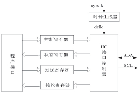
Figure 4 Overall block diagram of the I2C bus interface
Among them control register mainly realizes the storage of the control signal, utilize the control register, the host computer can control I2C bus interface. It consists of two 8-bit registers, one of which is used to store the number of bytes to be read/written, WRcnt. The other bits of bits 0 and 4 of the register are used to store the five operating modes of read/write, in which 00001 corresponds. Byte write, 00010 corresponds to page write, 00100 corresponds to immediate address read, 01000 corresponds to random address read, and 10000 corresponds to sequential address read. The 5th bit is used to store the read/write status signal WR, the 6th bit is used to store the start signal Start, and the 7th bit is used to store the reset signal Reset.
The status register mainly stores the working status of the bus. Using the status register, the host can obtain the status information of the I2C bus interface in real time. The lowest bit of the status register indicates that data can be read from the receive register (ie, Data_Read_Ok), and the second highest bit indicates that data can be written to the transmit register (ie, Data_Write_Ok).
The send register mainly implements the storage of data and addresses to be sent. The address stored in the transmission register mainly includes the slave address (Slave_Addr) and the byte address (Word_Addr).
The receive data register implements storage of data read from the I2C bus. The host can read the received data through this register.
The clock generator is used for the generation of the I2C bus interface controller clock.
The I2C interface controller is the core of the bus design. The main functions of the I2C bus are realized through the interface controller.
2.2 I2C Interface Controller
The I2C interface controller is the heart of the design and the most difficult part of the design. The I2C interface controller needs to realize the read/write of the slave, and it needs to generate the clock (SCL) and data (SDA) signals that meet the control timing requirements according to the information of the control register. Because the control sequence is correct or not directly related to the reliability of the control, the finite state machine can be used to design the interface controller. I2C bus timing control diagram shown in Figure 5.
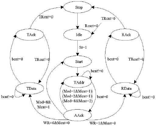
Figure 5 I2C bus timing state transition diagram
The idle state of the finite state machine is idle. When a reset signal (Reset=0) is received, the state machine enters the idle state. After the FPGA issues the start (St=1) command, the state machine will be in the Start state, on the clock line (SCL). ) and data line (SDA) issued on the start signal, and then the state machine to reach TAddr state, the host sends the device address and read and write mode information to the slave; when the output is complete, the host will receive the reply signal sent by the slave, and then state The machine will enter the corresponding state according to different working mode requirements. For example, the byte write and page write also need to output the byte address of the slave, and the response signal will only enter the write state. The random read will output the start signal and the slave again in addition to the address of the slave. The device address is then entered in the read state. Immediate address reads and sequential reads do not require the output byte address to enter the read state.
The data write mode can implement byte write and page write. After writing a byte of data, it will receive a response signal from the slave. If the number of bytes to be written is all written, the state machine enters the Stop state, otherwise it continues to write the next byte. The data read mode enables immediate address reads, random reads, and sequential address reads. After reading a byte of data, a response signal is sent. If all the numbers of bytes to be read have been read, the state machine enters the Stop state. Otherwise, the reading of the next byte is continued.
After the state machine enters the stop state, a stop signal is sent on the clock line (SCL) and the data line (SDA), and then the state machine enters the idle state.
2.3 I2C Interface Controller State Machine Code Design
The entire I2C interface controller state machine is composed of ten functional modules. Through the conversion between various modules, specific functions are implemented. The start module, end module, send data module, and receive data module are basic modules. Due to space reasons, The following is only the program code for implementing the above four basic module functions using Verilog HDL language. The declaration of the relevant variable is omitted here.
(1) Start module
This module is mainly used to achieve the start of bus communication control, when the clock bus (SCL) is high, the data bus (SDA) level changes from high to low, to achieve the beginning of bus communication. The code is described as follows:
Start:
Begin
Count=count+1;
Case(count)
1: SDA<=1;
2: SCL<=1;
3: SDA<=0;
4: SCL<=0;
5:
Begin
Count=0;
State<=TAddr;
End
Default: state<=Idle;
Endcase
End
(2) End the module
This module is mainly used to achieve bus communication stop control. When the clock bus (SCL) is high, the data bus (SDA) level changes from low to high, and the bus communication stops. The code is described as follows:
Stop:
Begin
Count=count+1;
Case(count)
1: SDA<=0;
2: SCL<=1;
3: SDA<=1;
4:
Begin
Count=0;
State<=Idle;
End
Default: state<=Idle;
Endcase
End
(3) Send data module
The send data module mainly realizes the function of writing data to the slave. Each time a byte data is written, when the number of bytes to be written is large, the module will be called repeatedly until all data is written from In the machine, the code is described as follows:
TData:
Begin
Count=count+1;
Case(count)
1: SDA< = data _
Write[bcnt];
2: SCL<=1;
3: SCL<=0;
4:
Begin
If(bcnt==0)
Begin
Bcnt=8;
Data_write_ok=1;
TRcnt=TRcnt-1;
State<=TAck;
End
Else
State<=TData;
Bcnt=bcnt-1;
Count=0;
End
Default: state<=Idle;
Endcase
End
(4) Receive data module
The receiving data module mainly realizes the function of reading data from the slave and completes the reading of one byte of data each time. When the number of bytes to be read is large, the module will be called repeatedly until all the data are read from the slave. Read it out and the code is described as follows:
RData:
Begin
Count=count+1;
Case(count)
1: SDA<=1'bz;
2: SCL<=1;
3: data_read[bcnt]=SDA;
4: SCL<=0;
5:
Begin
If(bcnt==0)
Begin
Bcnt=8;
TRcnt=TRcnt-1;
State<=RAck;
Data_read_ok=1;
End
Else
State<=RData;
Bcnt=bcnt-1;
Count=0;
End
Default: state<=Idle;
Endcase
End
3 I2C bus application
In the experiment, we verified the function of the I2C bus controller with the simulation timing of the AT24C02 memory chip reading and writing data. The simulation timing results meet the I2C communication standard. Download the program to the FPGA chip and run it. The communication data is correct and the circuit is stable and reliable. The I2C bus controller program performs logic synthesis in the Xilinx ISE 10.1 environment and uses ModelSim 6.2b for communication timing simulation. The simulation diagram is shown in Figure 6 and Figure 7.
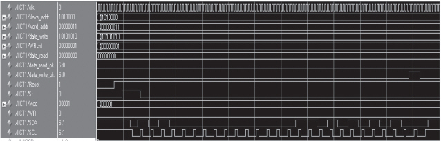
Figure 6 Simulation timing waveform of byte write mode
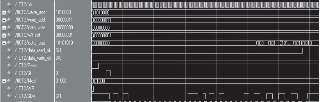
Figure 7 Simulation timing waveforms for random address read operation mode
Fig. 6 is the simulation waveform diagram that the host writes, mainly realizes the byte write sequence simulation of AT24C02 memory. The simulation in the figure is to write 1 byte data of AAH to a memory cell whose device address is 50H and whose byte address is 03H. From the timing relationship of the simulation, it can be seen that the host writes the slave address and data and the timing of the slave response signal is correct.
Figure 7 shows the simulation waveform of the host randomly reading data from the slave. Mainly realizes the timing simulation of random address reading of AT24C02 memory. The simulation process reads out the previously written 1-byte data, and the read result is exactly the same as that written. From the timing relationship of the simulation, it can be seen that the host writes the slave address, reads out the data, and the timing of the master acknowledgement signal is correct.
In practical applications, the I2C bus controller can implement read and write operations on the five operating modes of the AT24C02 chip, and can simultaneously perform data read and write operations on the AD5248 digital potentiometer.
4 Conclusion
Based on the I2C bus communication protocol, this paper designs the I2C controller in a state machine mode, and analyzes some basic modules. At the same time, the timing of the read/write status of the controller is verified by the AT24C02 chip. The results show that the I2C bus The signal complies with the I2C communication standard, and downloading to the FPGA can fully realize the reading and writing of the chip with the I2C communication protocol.
Due to the flexibility of FPGA field programmable features in programming and debugging. The design can generate an IP core and embed it into an FPGA-based system design that can read and write IC chips in the I2C bus. It can avoid the repeated development of different products and improve the design efficiency of the system. Reduced product development cycles and costs.
Magnetic Transducer External Drive Type
The magnetic transducers (External Drive Type) are versatile and customizable to different physical sizes, housings, mounting options, power consumptions. Our magnetic transducers are engineered to be used with an external drive circuit. This allows our customers the flexibility to design and customize the circuitry to meet their needs. External circuitry allows different frequency ranges to be used to create multiple sounds through excitation waveform. Our magnetic transducers come in a slim-line profile and are a cost-effective solution. Our extensive capabilities make our magnetic transducers an excellent solution for high/low tones, siren, and chime sounds.
Piezoelectric Buzzer,Passive Magnetic Buzzer,External Drive Buzzer,Magnetic Transducer External Drive Type
Jiangsu Huawha Electronices Co.,Ltd , https://www.hnbuzzer.com