Description: When switching between rows in a single bank, each time a Row is opened, after a write operation, another Row must be reopened to perform the Row write operation. There are time gap requirements for the two Row open operations, and there is also a time gap requirement for opening the Row to Write operation. Therefore, when a single bank is switched, the bandwidth utilization is extremely low. In the figure, 8 data is valid for each write operation, and the last 8 data are invalid. Therefore, in the time taken by a write operation, the effective time is only 8 ns, and the invalid time is 60 ns, resulting in a total bandwidth utilization of only 8/68 = 11.8%.
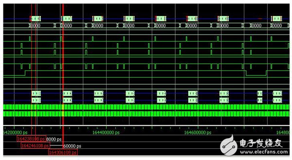
Figure 2 Single-bank multi-line switching timing diagram
Two. Two banks do not wrap smooth transition testDescription: Firstly write 8 times in the same Row of Bank0 and then transfer to the same Row of Bank1 for 8 consecutive writes. It is possible to open a Row of Bank1 during the write operation of Bank0 without affecting the write operation of Bank0. Since enough time is required to open Bank1, after the write operation of Bank0 is finished, it can be smoothly and smoothly transitioned to the write operation phase of Bank1 without waiting in the middle. The bandwidth utilization of this mode of operation is close to 100%, regardless of the bandwidth consumption of the DDR3 timing charging and the bandwidth consumption of the read and write switching. This application mode is well suited for continuous caching of data, maximizing bandwidth utilization.
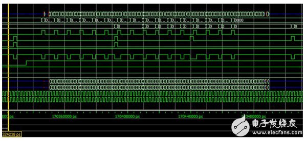
Figure 3 Two banks do not wrap smooth transition timing diagram
Silicone Daily Necessities,Silicone Products,Silicone Molds,Silicone Rubber Part
Nantong Boxin Electronic Technology Co., Ltd. , https://www.ntbosen.com