The semiconductor industry is ushering in a new era of next-generation memory technologies. Several major changes are taking shape. This includes the emergence of Magnetic Random Access Memory (MRAM). In a few related articles, I will introduce the background to promote the adoption of MRAM, highlight some of the challenges that were faced in the initial phase, and discuss the progress in the commercial feasibility of STT MRAM.
Applied Materials has provided a number of important innovations for the manufacture of STT MRAMs, including innovations in PVD based on the Endura platform and special etching techniques. Utilizing these new technologies and machining and testing device arrays with the facilities of the Meydan Technology Center, we verified the performance and scalability of the STT MRAM.
Today, in addition to logic components and other specialized circuit elements, a typical microcontroller (MCU) includes SRAM used as a working memory and a flash memory used as a storage memory. The current flash memory problem encountered by the industry is to minimize the impact of floating gate (FG) manufacturing processes on the performance of logic gates (Figure 1). For this reason, manufacturers often use up to 10 additional mask layers, which inevitably increases their complexity and cost. At the 28nm node, the logic portion of the process will be migrated to the high-k gate dielectric/metal gate (HKMG), which will lead to more complex process integration due to the limited thermal budget of HKMG.

Figure 1: MCU Integration with Flash (left) and STT MRAM (right)
On the other hand, integrating a spin-transfer torque MRAM (STT MRAM) in the back-end process (BEOL) is relatively easy, requiring only 3 additional masks (Figure 1). In addition, flash memory consumes more energy than STT MRAM. The promising features of STT MRAM (fast, non-volatile, low power, and easy implementation of BEOL integration at low temperatures) led most major logic and memory vendors to gradually develop STT MRAM technology. In addition to MCUs, STT MRAMs are also being developed to replace SRAMs because they can achieve higher densities compared to SRAMs. They are used as the last-level cache for 10nm nodes.
Each memory cell of the STT MRAM consists of a magnetic tunnel junction (MTJ), the most basic form of which is a thin dielectric tunneling barrier film sandwiched between two magnetic films (about 10-30 Ã… thick CoFeB). 10Ã… thick MgO) composition. There are actually many additional thin film layers in the MTJ stack (see Figure 2a in the example) and have been manufactured as read sensors in hard disk drives (HDDs) since 2007.
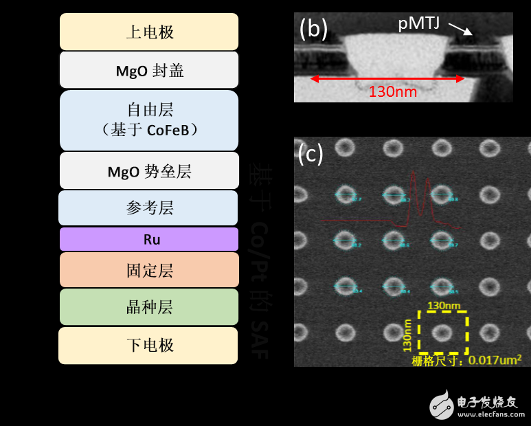
Figure 2: (a) pMTJ stack details, (b) and (c) show cross-sectional and top views of the pMTJ array
However, the requirements for the individual MTJ devices in the HDD and the vertical MTJ (pMTJ) device array in the STT MRAM are completely different. Innovations in the pMTJ thin-film stack deposition and etching process equipment are critical to manufacturing density/performance-competitive STT MRAMs. In addition, the initial production of wafers from the memory manufacturer that will be producing STT MRAM is 10-20 times higher than that of HDD head manufacturers. Therefore, when designing equipment, equipment uptime is a key factor to consider.
Applied Materials has developed a multi-cathode PVD chamber and a variety of in-situ thermal chambers on the company's Endura platform for pMTJ stack layer deposition (multilayer films with controllable microstructure, clean interface, and sub-Ã… precision). In addition, special etching techniques for nonvolatile magnetic materials in dense arrays have also been developed for etching pMTJ arrays. [1]
To evaluate the performance of the pMTJ deposition and etching equipment, a 1R pMTJ array test chip was designed and manufactured at the Meydan Technology Center. The minimum memory cell size of 130nm x 130nm (Figure 2) is equivalent to 22F2 at the 28nm node, which corresponds to approximately 1Gb density. These test chips have been subjected to electrical analysis at Qualcomm and the results were also published in the 2015 and 2016 International Electronic Components Conference (IEDM). [2, 3] These results discussed in the following paragraphs focus on the performance of pMTJ arrays manufactured using the Endura PVD system and special etching techniques.
A key performance indicator is the TMR% (tunnel magnetoresistance) of the etched MTJ array. For a pMTJ array with a pitch of 130 nm and a 50 nm diameter, the average TMR is about 150% (Figure 3). Resistance (RP) Sigma / Average "8%. Both of these values ​​indicate that the etch damage during the etching process is minimal. By optimizing the free layer (FL) material in the pMTJ stack, P-AP toggle currents (35ns flipping pulses) as low as about 90uA can be obtained in the array (Figure 4).
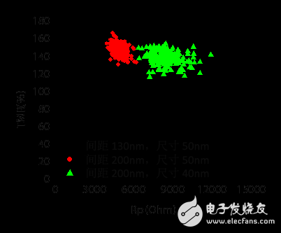
Figure 3: TMR percentage plots with different array spacings and CDs
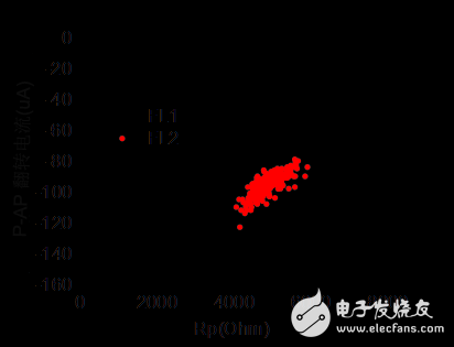
Figure 4: Reduction of flipping current through free layer (FL) optimization
Finally, by optimizing the device hardware design of the MgO deposition chamber, as shown in Figure 5, the breakdown voltage of the about 10 Å MgO tunnel barrier layer can be significantly increased from about 1.2 V (standard) to about 1.5 V (improved). As demonstrated in our work, this is critical for improving durability to “1015 write cycles. [3] I will explore this issue further in my next blog.
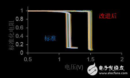
Figure 5: MgO VBD improvements through process and device hardware optimization
1. Lin et al., IEEE Trans of MagneTIcs, vol. 51 2015 p4401503
2. Park et al., 26.2, IEDM 2015
3. Kan et al., 27.4, IEDM 2016
1. Lin et al., IEEE Trans of MagneTIcs, vol. 51 2015 p4401503
2. Park et al., 26.2, IEDM 2015
3. Kan et al., 27.4, IEDM 2016
Mahendra Pakala
Mahendra Pakala is responsible for the development of STT MRAM, including a technology roadmap for the manufacturing process of magnetic tunnel junction stacks and MTJ arrays. He holds a Ph.D. in Materials Science from the University of Cincinnati and has obtained more than 30 patents.
Absolute Linear Encoders,Custom Absolute Encoder,Rotary Encoder Magnetic,Miniature Absolute Encoder
Yuheng Optics Co., Ltd.(Changchun) , https://www.yuhengcoder.com