The LPC54102 MCU is an ARM Cortex-M4-based embedded application microcontroller. These devices include an optional ARM Cortex-M0+ coprocessor, 104 KB of on-chip SRAM, up to 512 KB of on-chip flash, five general-purpose timers, a state-configurable timer with PWM capability (SCTImer/PWM), and an RTC/ Alarm timer, a 24-bit multi-rate timer (MRT), a repeat interrupt timer (RIT), a windowed watchdog timer (WWDT), four USARTs, two SPIs, three high-speed slaves The mode of the ultra fast mode I 2 C bus interface and a 12-bit 5.0 MSPS ADC.
Main parameters: 32-bit ARM Cortex-M4/M0+ MCU; 104 kB SRAM; 512 kB flash, 3 x I2C, 2 x SPI, 4 x USART, 32-bit counter/timer, SCTImer/PWM, 12-bit 5.0 MSPS ADC
Lpc54102 features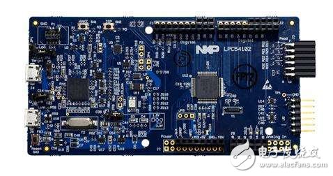
Dual processor cores: ARM Cortex-M4 and ARM Cortex-M0+. The M0+ core operates at the same frequency as the M4 core. Both cores can operate up to 100 MHz.
ARM Cortex-M4 core (r0p1 version):
1. The ARM Cortex-M4 processor runs at up to 100 MHz and uses the same clock as the Cortex-M4.
2. Floating point arithmetic unit (FPU) and memory protection unit (MPU).
3, ARM Cortex-M4 built-in nestable interrupt vector controller (NVIC).
4, non-maskable interrupt (NMI) input, a variety of interrupt sources to choose from.
5, serial line debugging, with 8 breakpoints and 4 observation points. Includes serial line output for enhanced debugging.
6, system timer.
ARM Cortex-M0+ core (r0p1 version):
1, ARM Cortex-M0+ processor, running at up to 100 MHz.
2, ARM Cortex-M0+ built-in nestable interrupt vector controller (NVIC).
3. Non-maskable interrupt (NMI) input, a variety of interrupt sources are available for selection.
4, serial line debugging, with four break points and two observation points.
5. System timer.
On-chip memory:
1. Up to 512 kB on-chip flash programmable memory with flash accelerator and 256-byte page erase and write function.
2. A total of 104KB of SRAM is included: up to 96 kB of continuous main SRAM and an additional 8 kB of SRAM.
ROM API support:
1. Flash in Application Programming (ISP) and In-System Programming (IAP).
2. Power control API.
Serial interface:
1. Four USART interfaces supporting synchronous mode and 32 kHz mode for wake-up from deep sleep and power-down modes. The USART has FIFO support from the system FIFO and shares a fractional baud rate generator.
2. Two SPI interfaces, each with four slave selects and flexible data configuration. The SPI has FIFO support from the system FIFO. The slave function wakes up the device from deep sleep and power-down modes.
3, three I 2 C bus interface, support fast mode and ultra fast mode, data rate up to 1 Mbit / s, multi-address recognition and monitoring mode. Each I 2 C bus interface also supports high speed mode (3.4 Mb/s) as slave mode. The slave function wakes up the device from deep sleep and power-down modes.
Digital peripherals:
1, DMA controller, with 22 channels and 20 programmable triggers, access to all memory and DMA-enabled peripherals.
2. Up to 50 general purpose input/output (GPIO) pins. Most GPIOs have configurable pull-up/pull-down resistors, programmable open-drain mode, and input inverters.
3. The GPIO registers are located on the AHB to support fast access. The DMA supports GPIO ports.
4. Up to 8 GPIOs (pin interrupts) can be selected as edge trigger type (rising edge or falling edge, or both) interrupt request or level trigger type (active low or active high) interrupt request. In addition, up to 8 GPIOs can be selected for a Boolean expression and pattern matching engine data blocks can be used to generate interrupts.
5. Two sets of GPIO interrupts (GINT) support interrupts based on input state logic (AND/OR) combination.
6, CRC engine.
Timer:
1, 5 32-bit standard general-purpose timers/counters, 4 of which support up to 4 acquisition inputs and 4 comparison outputs, PWM mode and external count input. A specific timer event can be selected to generate a DMA request. The fifth timer has no external pin connections and can be used for internal timing operations.
2. One state configurable timer/PWM (SCT/PWM) with 8 inputs (6 external inputs and 2 internal inputs) and 8 output functions (including capture and match). Inputs and outputs can be connected to or from external pins, or can be connected to or from internal selected peripherals. Internally, the SCT supports 13 acquisitions/matches, 13 events and 13 states.
3. 32-bit real-time clock (RTC) running at 1 S resolution in the always-on power domain. Timers in the RTC can be used to wake up all low power modes (including deep power down mode) with 1 ms resolution.
4. Multi-channel, multi-rate 24-bit timer (MRT) for repeated generation of interrupts at up to four programmable fixed rates.
5. Windowed watchdog timer (WWDT).
6. The ultra-low-power Micro-TIck timer, which operates from the watchdog oscillator, can be used to wake the device from low-power modes.
7. Repeat Interrupt Timer (RIT) for debugging time stamps and general purpose.
   8. Analog peripherals: 12-bit 12-channel analog-to-digital converter (ADC) supporting 5.0 MSPS. The ADC supports two independent conversion sequences.
Clock generation:
1, 12 MHz built-in RC oscillator.
2. The clock frequency of the external clock input is up to 25 MHz.
3. Internal low power watchdog oscillator (WDOSC) with a nominal frequency of 500 kHz.
4, 32 kHz low power RTC oscillator.
5. The system PLL allows the CPU to run at the maximum CPU speed. It can be operated from the internal RC oscillator, external clock input CLKIN or RTC oscillator.
6. Clock output function for monitoring the internal clock.
7. A frequency measuring unit for measuring the frequency of on-chip and off-chip clock signals.
Energy saving mode and wake up:
1. Integrated PMU (Power Management Unit) for reducing power consumption.
2, reduce power consumption mode: sleep, deep sleep, power down and deep power down.
   3. Wake up from deep sleep mode and power down mode via activity on the USART, SPI, or I 2 C peripherals.
4. Wake up from sleep, deep sleep, power down and deep power down mode via RTC alarm.
1.62 V to 3.6 V single supply.
Power-on reset (POR).
Brownout detection (BOD) with independent thresholds for interrupts and forced resets.
Support for JTAG boundary scan.
A unique serial number (128 bits) that can be used for chip identification.
The operating temperature range is −40 °C to 105 °C.
Available in a 3.288 mm x 3.288 mm WLCSP49 package and LQFP64 package.
Phone Stand Holder Adjustable,Cell Phone Stand Holder,Phone Stand Holder Desk,Phone Stand Holder Hand,etc.
Shenzhen Chengrong Technology Co.ltd is a high-quality enterprise specializing in metal stamping and CNC production for 12 years. The company mainly aims at the R&D, production and sales of Notebook Laptop Stands and Mobile Phone Stands. From the mold design and processing to machining and product surface oxidation, spraying treatment etc ,integration can fully meet the various processing needs of customers. Have a complete and scientific quality management system, strength and product quality are recognized and trusted by the industry, to meet changing economic and social needs .

Phone Stand Holder Adjustable,Cell Phone Stand Holder,Phone Stand Holder Desk,Phone Stand Holder Hand
Shenzhen ChengRong Technology Co.,Ltd. , https://www.dglaptopstandsupplier.com