0 Preface
Data acquisition is an important part of signal analysis and processing. The fast and reliable experimental data in the missile semi-physical simulation process plays an important role in improving simulation accuracy. Traditional digital data acquisition systems are intertwined with various digital and analog signals. The corresponding peripheral circuits are large and the interfaces are complex. It takes up a large space of the circuit board and cannot meet the miniaturization requirements of the system, and the hardware cost is also high. When the system performance index changes, the corresponding functional circuit and its corresponding isolation, filtering and other circuits and related procedures must be changed. This kind of structure that leads to the whole body leads to the system's low scalability and the system's versatility. On the other hand, early data acquisition systems are mostly based on complex programmable logic devices (CPLDs), and the sampling speed and accuracy of the data are not very high.
With the development of integrated circuit technology, NI's FPGA board has gained more and more applications with its IO pin, rich on-chip resources, flexible structure, and embedded controller. Its nanosecond level Speed ​​can greatly increase the speed and accuracy of data sampling. As a result, data acquisition systems based on National Instruments' FPGA boards can monitor semaphore changes in real time and quickly compared to traditional data acquisition systems. Moreover, the system has simple structure, short development cycle, high reliability and good real-time performance, and can complete the data collection task of missile semi-physical simulation, and has strong versatility.
1 system design
The main purpose of designing the data acquisition system is to collect the rudder signal of the missile in the semi-physical simulation system of the missile and transmit it to the host computer for calculation and simulation. The system has better scalability, can flexibly adapt to different applications, and has strong versatility.
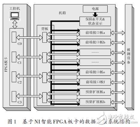
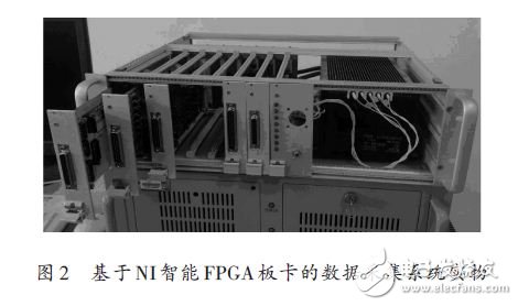
The system structure diagram is shown in Figure 1. The physical diagram of the system is shown in Figure 2. The front-end interface circuit board with data acquisition function and data communication function is integrated in one chassis, and connected on the same backplane by an independent power supply. powered by. The four interfaces on the backplane are connected to the FPGA board installed in the industrial computer through the NI dedicated data cable. The data acquisition and control signal transmission between the industrial computer and the hardware-in-the-loop hardware system is realized through the FPGA board and the LabVIEW graphical programming development platform.
Breadboard Jumper Wire,Breadboard Wires,Breadboard Cables,Breadboard Jumper Cables
Cixi Zhongyi Electronics Factory , https://www.zypcbboards.com