CDMA / EVDO and WCDMA / HSPA are the two most widely deployed technologies in 3G. These two technologies depend on code division multiple access (CDMA) digital wireless technology, allowing many users to effectively use voice and data communications in the same radio frequency spectrum. CDMA is a spread-spectrum radio frequency communication that relies on a unique "cut code" to be allocated to each user to distinguish other users in the same RF spectrum. Spectrum expansion increases channel capacity and allows multiple users to use the operator ’s full bandwidth. CDMA / EVDO network operators use 1.25MHz, while WCDMA / HSPA networks use the wider 5MHz. The data transmission rate can further increase high-order modulation in the wireless network to provide a better user experience and wireless data.
Multi-band CDMA and WCDMA mobile phones require greater RF design work to provide sufficient output power and ensure the normal operation of linearity and efficiency in each frequency band. The design usually includes a power amplifier and duplex for each frequency band, RF filters and switches to match multiple RF inputs to a single antenna. In order to reduce the complexity of multi-band mobile phone design, ANADIGICS has developed dual-band CDMA and WCDMA power amplifier modules. By integrating two power amplifier modules in a single package, compared with the previous DC and RF signal line design using two separate power amplifiers, the board area can be effectively reduced. This article will describe the typical application of dual-frequency power amplifier module in CDMA / EVDO and WCDMA / HSPA mobile phone design.
This article will focus on the design and application of ANADIGICSAWT6221 in UMTS band 2 and band 5, dual band WCDMA / HSPA mobile phones. The AWT6221 of ANANDIGICS has won the Outstanding Achievement Award (2) for Information Application, Communication Technology Innovation, the EDN Innovation Award, and the Excellent Product Award for Communication and Network issued by the Ministry of Industry and Information Technology of China.
AWT6221 dual-frequency power amplifier greatly reduces the average current power consumption by up to 75% and increases the talk time by up to 25%.
ANADIGICS 'HELP3 â„¢ power amplifier, such as the AWT6221 power amplifier, uses the company's unique InGaP-Plus â„¢ technology, integrating bipolar and field effect transistor (FET) devices in the same InGaPGaAs bare die. With an optional bias mode, the HELP3 â„¢ power amplifier exhibits the best efficiency in the low range and mid-range output power level. The AWT6221 smart bias circuit reduces current consumption to eight milliamps at low power levels-the best in the world. By integrating two independent power amplifier chains, the ultra-mini AWT6221 provides excellent performance in these two frequency bands and saves printed circuit board area. (figure 1)
ANADIGICS provides dual-band WCDMA / HSPA power amplifier modules for popular combined frequency bands and dual-band power amplifier modules for CDMA / EVDO applications. For more information, please refer to ANADIGICS (). ANADIGICS has developed reference design products to help customers achieve their design goals faster and easier. In this article we will describe the advantages of the AWT6221 (Figure 2) reference design.
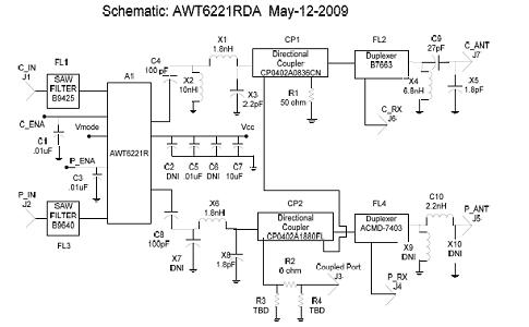
figure 1
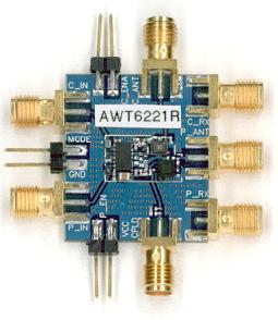
figure 2
AWT6221 is developed for dual band WCDMA / HSPA mobile phone UMTS band 2 (824-849MH) and band 5 (1850-1910MHz). 3GPP technology regulates the level 3 power of user equipment, which must meet or exceed these minimum performance levels (3)
• Maximum output power: + 24dBm + 1 / -3dBm
• Adjacent channel leakage power ratio (ACLR) +/- 5MHz: -33dBm
• Adjacent channel leakage power ratio (ACLR) +/- 10MHz: -43dBm
• Maximum harmonic emission specified frequency: 30–1000MHz: -36dBm / 100kHz
o Between 1-12.75GHz: -30dBm / 1MHz
o Between 869–894MHz: -60dBm / 3.84MHz
o Between 1930-1990MHz: -60dBm / 3.84MHz
o Between 2100-2170MHz: -60dBm / 3.84MHz
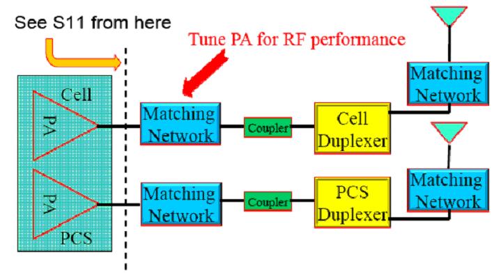
The frequency division duplex system of most CDMA and WCDMA networks allows different radio frequency bands to be allocated to uplink (from mobile to base station) and downlink (from base station to mobile) at the same time. Duplexers are used in mobile devices to allow UL and DL to utilize a single antenna. In UMTS Band 2, we chose Avago Technology's micro-FBAR duplex high-Q response ACMD-7403. For Band5, we choose Epcos low loss SAW duplex B-7663. The reference design also includes the coupled AVX of the CP402A thin film power directional coupler, which provides the required RF power for many top 3G chipsets.
The development of the AWT6221 reference design started with the further coupling of the power amplifier and the measurement of duplex S-parameters. In this measurement, zero-ohm resistance is used to shorten the matching components on the circuit board (Figure 3).
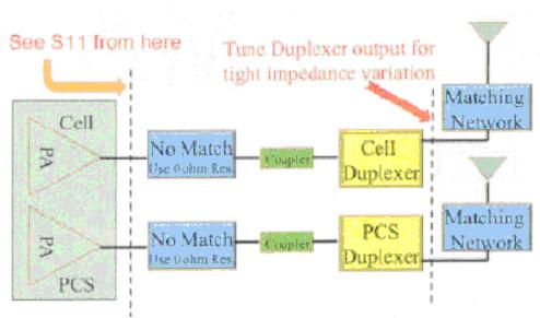
image 3
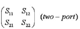
The S parameter describes the voltage signal reflected by each port network of the N port. The subscript of the first number refers to the response port, while the second number refers to the event port. Therefore S21 refers to the reaction caused by the signal terminal 1 at port 2. The S parameter comes from a matrix port with equal number of rows and columns. The parameters along the diagonal of the S matrix are called reflection coefficients, and the diagonal S parameters are called transmission coefficients because they only occur at a single port. The two-port network of the S matrix is ​​shown in the table below:
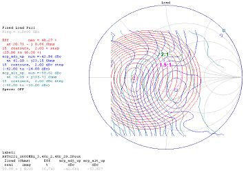
The reflection coefficient (S11) is tested against the frequency range of the RF path of Band 2 and Band 5. The power amplifier forms a series of impedance changes from the output of the non-conforming circuit, and the results are shown in the Smith table (Figure 4, Figure 5).
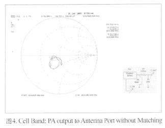
Figure 4
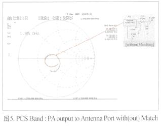
Figure 5
For any power amplifier, the output impedance has a significant impact on operation, and strongly affects the power transferred to the antenna, linearity (ACLR), and operational efficiency. Power amplifiers from manufacturers like ANADIGICS can help engineers balance these load traction information. The optimal output impedance will be affected by the characteristics of other RF chain components, such as duplexers and switches are not always 50Ω. The advantages and operating temperatures of the variable frequency duplex feature band are particularly challenging in the development of well-developed WCDMA radio frequency designs. (Figure 6, Figure 7)
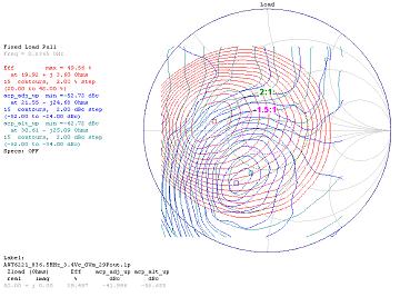
Image 6
Picture 7
The next step in developing the AWT6221 reference design is to match the impedance of the duplex antenna to minimize the frequency of impedance changes in each frequency band. Although the simple two-components theoretically have excellent performance over narrow-band frequencies, obtaining good performance in a wider bandwidth, and compensating for production tolerances and temperature changes, or predictable variables caused by voltage often require additional Elements of compliance. 3 The results of the component selection for the two frequency bands are shown in the Smith chart. The matching network greatly reduces the impedance variable under duplex, thereby simplifying the remaining circuits that can be met. (Figure 8, Figure 9)
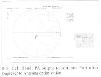
Figure 8
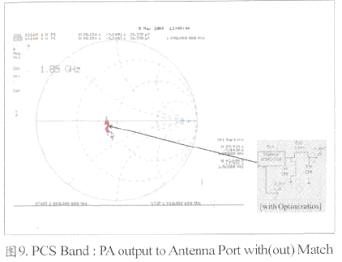
Figure 9
Picture 10
The next step in developing the AWT6221 reference design is the pairing between power amplifier and coupler + duplex. Again, for Band 2 and Band 5, the reflections for the measurement of the frequency range of the RF path (S11) (Figure 10); it is ultimately used to formulate a minimum impedance variable that can be used in WCDMA operation to optimize A network for power amplifier performance requirements. As before, a 3-element network can achieve good performance; the results are shown in the Smith charts in Figures 11 and 12.
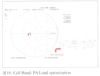
Picture 11

Picture 12
The final product reference design meets the requirements of WCDMA in Band 2 and Band 5 at room temperature. In addition, the matching network keeps the performance specifications within all expected ranges, and minimizes the changing frequency, temperature, and power supply voltage (Figure 13, Figure 14).
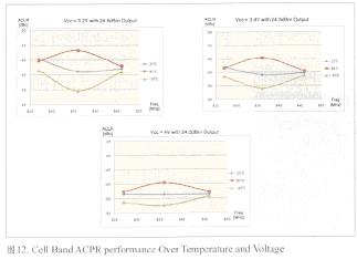
Figure 13
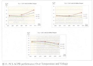
Figure 14
The reference design discussed in this article can provide a useful starting point for the development of newly designed 3G mobile phones, data cards, wireless modems, and other WCDMA / HSPA devices. When developing new designs, engineers need to consider the important functional requirements of the design and consider changing the matching network discussed here to achieve the best trade-offs in output power, linearity, efficiency, and other RF parameters. Reviewing the load pull of each power amplifier will help determine the optimal output impedance matching point that may not be 50Ω. The engineer must also consider the variable RF path and network selection of each part, reduce the antenna output variables, and not exceed the expected use temperature, frequency and power supply voltage, so that all RF parameters are maintained at acceptable levels. Finally, it will be important to control the reflection (return loss) of the power amplifier to avoid causing instability or oscillations in the circuit.
ANADIGICS 'AWT6221 is one of the dual-frequency power amplifier series in 3G mobile phones and data devices. At present, ANADIGICS 'dual-band power amplifier products are listed as follows, and new designs are also being developed. For more information on these products, please contact ANADIGICS.
• AWT6221: WCDMA / HSPAHELP3 ™ is suitable for dual-mode PA in UMTS band 2 and 5
• AWT6222: WCDMA / HSPAHELP3 ™ is suitable for dual-mode PA in UMTS band 1 and 6
• AWT6224: WCDMA / HSPAHELP3 ™ is suitable for dual-mode PA in UMTS band 1 and 8
• AWT6321: CDMA / EVDOHELP2 ™ is suitable for dual-mode PA in cellular and PCS bands
Aluminum Extrusion Radiator,Led Heat Sink Aluminum,Heatsink Extrusion Profiles,Aluminium Heatsinks
Original Electronics Technology (Suzhou) Co., Ltd. , https://www.original-te.com