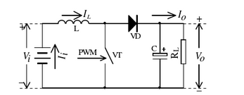
The boost converter is called a parallel switching converter. The difference from the buck converter is that the boost inductor is at the input (switch) and the buck inductor is at the output. The output voltage Vo of the boost converter is always greater than the input voltage Vi. The explanation is relatively simple. When the switch tube is turned on, the diode D is turned off, and the node voltage between the inductor L and the switch tube is 0. When the switch tube is turned off, the potential across the inductor L reverses, so the node voltage between the inductor L and the switch tube is greater than the input voltage Vl, and the inductor current flows through the diode D, making Vo greater than Vi. It can be proved that Vo=Vi*[T/(T-Ton)], T is the switching pulse period, and Ton is the on-time.
The working principle of boost converterThe main relationship and critical inductance of Boost converter when working in CCM and DCM
According to whether the minimum current flowing through the inductor is zero (that is, whether the inductor current is intermittent during S off), the Boost switch can also be divided into two modes: continuous conduction mode (CCM) and discontinuous conduction mode (DCM) . For a given switching frequency, load resistance, input and output voltage, Boost converter has a critical inductance Lc, when L>Lc, the converter is in CCM: and when L
The basic working principle is that in the case of input voltage changes, internal parameter changes and external load changes, the control circuit performs closed-loop feedback through the difference between the controlled signal and the reference signal, and adjusts the on (or off) time of the main circuit switch tube. Make the output voltage or current of the switching converter relatively stable.
In order to analyze the steady-state characteristics and simplify the process of deriving the formula, the following two assumptions are made:
(1) The switch tube and the freewheeling diode are ideal components. That is, it can be turned on or off instantly, and the voltage drop is zero when it is turned on, and the leakage current is zero when it is turned off.
(2) Inductors and capacitors are ideal components. The inductance I is made in the linear region without saturation, the parasitic resistance is zero, and the equivalent series resistance (ESR) of the capacitor is zero.
Working mode of boost converterBoost DC-DC converter is also called Step Up Converter, and its circuit topology is shown in Figure 2.1. The basic circuit of BoostDC-DC converter is composed of power switch tube VT, freewheeling diode VD, energy storage inductor L, output filter capacitor C and so on. Because the switching speed of the MOSFET tube is relatively fast and the control logic is relatively simple, the switching tube VT generally adopts a MOSFET tube.
During the switch-on period of the switch tube VT, the current in the inductor rises: during the switch-off period of the switch tube VT, the inductor current drops. If the current in the inductor drops to zero during the cut-off period of the switching tube VT, and the energy stored in the inductor is also zero during the remaining time of the cut-off period, the switching power supply is said to work in the discontinuous inductor current mode (Discontinuous ConducTIon Mode, DCM); otherwise, it works in the inductor current continuous working mode (ConTInuousConducTIon Mode, CCM)". The two working modes of the Boost DC-DC switching converter are analyzed separately to facilitate system design.
Assume that the input voltage range of the Boost DC-DC switching converter is [V.min, V.max], and the load resistance range is [R min, RL.max]. On the RL-V; plane, the working range of the switching converter corresponds to a rectangle. According to the expressions of the critical inductance Lc of each switching converter CCM and DCM and the critical inductance Lk of CISM and IISM, the curve described by it is drawn. The RL-V; plane can be divided into two parts: CCM and DCM and CISM and IISM, as shown in Figure 2.5, where LcB
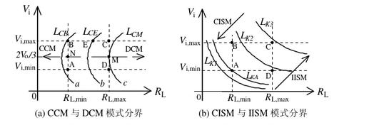
It can be seen from Figure 2.5 that for the Boost DC-DC converter, the critical inductance LK of CISM and IISM has a monotonic relationship with the input voltage and load resistance, while the critical inductance Lc of CCM and DCM is not monotonous with the input voltage and load resistance. relationship. On the RL-V; plane, with different inductance values, Boost converter I works in different modes 34.12-131
Related Links
Briefly describe the role of pwm converter
Boost converter DC converter, boost DC converter design
French Power Strip,Surge Protector Power Strip,Power Strip With Flat Plug,Overload Protector Power Strip
CIXI KYFEN ELECTRONICS CO.,LTD, , https://www.kyfengroup.com