In order to satisfy that the relevant pins are in a certain state and simplify the design during the system power-on process, first ensure that the 3.3V voltage of all modules (including VDDIO, VDD3VFL, VDDA1/VDDA2/VDDAIO/AVDDREFBG) is supplied first, and then 1.8 V or 1.9 V voltage. It is required that the voltage of 1.8 V or 1.9 V (VDD/VDD1) cannot exceed 0.3 V before the VDDIO voltage reaches 2.5 V. Only in this way can it be ensured that during the power-on process, the core is powered on after all I/O states are determined, and the processor module is in a correct reset state after power-on. The power-on sequence is shown in Figure 1.
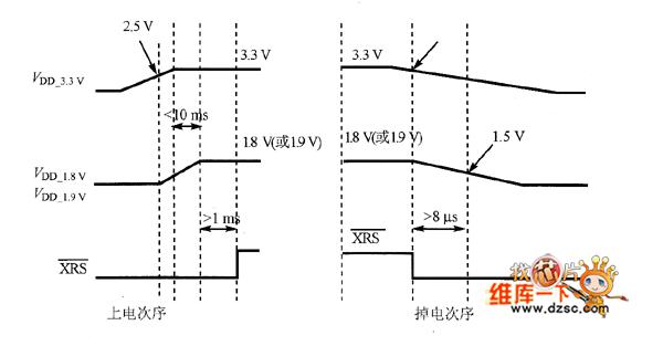
Figure 1 281x processor power-up/power-down sequence sequence
During the power-down process, before VDD drops to 1.5 V, the reset pin of the processor must be inserted into a low level of at least 8 μS. This helps to reset the on-chip Flash logic before VDDIO/VDD is powered down. Therefore, the reset output of the LDO is generally used as the reset control signal of the processor during power supply design. The principle of power supply is shown in Figure 2.
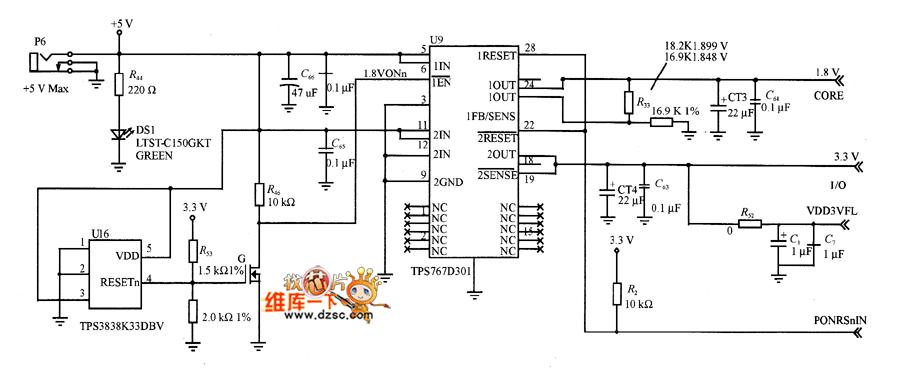
Figure 2 281x processor power supply principle diagram
Indoor Outdoor Fiber Optic Cable,Indoor Outdoor Fiber,Indoor Fiber Cable,Indoor Fiber Optic Cable Types
Zhejiang Wanma Tianyi Communication Wire & Cable Co., Ltd. , https://www.zjwmty.com