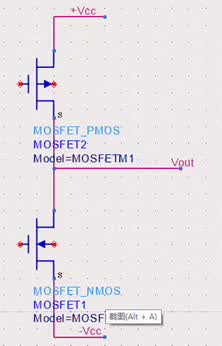
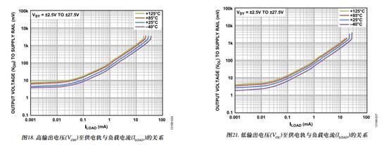
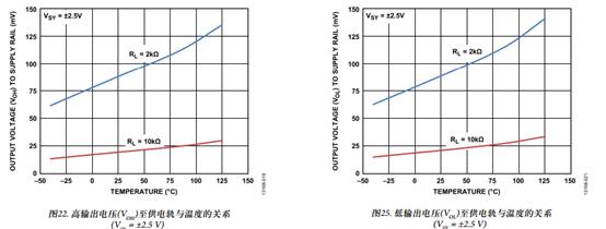
Since the MOS transistor has an on-resistance, when a current flows, a voltage drop is caused. Therefore, when the load is larger, the on-state voltage drop is larger, and the output voltage is less likely to reach the rail.
Therefore, the rail-to-rail op amp is not completely able to make the output reach the power supply value. When it is used, it is necessary to look at the relationship between the load and the temperature (affecting the resistance of the on-resistance) to determine how much the output can reach.
2. The input bias current of the op amp ten pits can not be ignored
A voltage divider circuit is designed. In theory, input 1V, output 2V, but one test, always more than 6,7 mV. This is to enter the 12-bit 3V range ADC, but to eat more than 600 yards. Point solution?
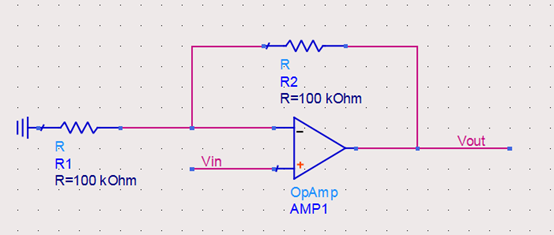
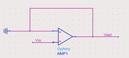
The positive input and reverse inputs of the op amp resulted in input bias currents at the two inputs due to TVS leakage current and tube input bias current (and because no one device is identical to the other, both The input bias currents are not the same); these two bias currents form a bias voltage with the external resistor and output to the back end, creating an error . If you accidentally choose a BJT-based op amp, it has a large input bias current, which will cause a large back-end error. As shown in the figure below, this kind of op amp is really "stopping at the big, it is simply awkward."

The following assumes that the input bias currents of the two inputs are the same.
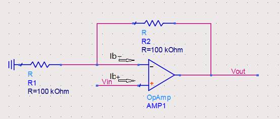
For the forward input, Ib+ brings the bias voltage to be almost equal to 0, and for the inverting input, Ib- brings the bias voltage equal to 350mV (when calculating, assume Vout is grounded, equivalent to R1/ /R2). Therefore, what is needed is to add a resistor to the forward input to compensate for the error caused by the inverting input.


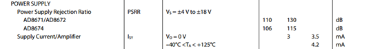
Even if the supply voltage changes between 4.5V and 5.5V, the effect of the power supply on the output of the op amp is only 10nV.
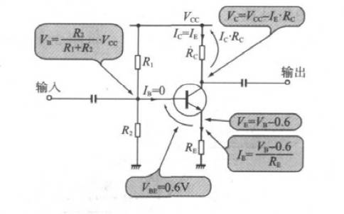
Unfortunately, this indicator refers to the DC change of the power supply voltage, and does not include changes in the power supply voltage exchange (such as ripple). In the case of AC, this indicator will be greatly deteriorated. What is mentioned in Spec. is only the DC change. The change of communication is shown in the figure below. Under normal circumstances, the non-senior engineers treat the illustrations smoothly and slid over.
If the op amp circuit uses a switching power supply and does not perform decoupling and filtering well, the input accuracy of the latter stage will be greatly affected. Look at the exchange PSRR of the same op amp.
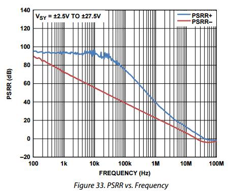
For the 500kHz switching frequency ripple, PSRR+ deteriorates to only 50dB. Assuming a ripple size of 100mV, the effect on the post-stage will deteriorate to 0.3mV. For many small signal acquisition applications, this error is unacceptable. Therefore, some applications even make a low-pass filter at the op amp power inlet (note the resistor power and resistor thermal noise ).
4. The compensation capacitor of the operation of the ten pits
In the past, an "old engineer" told me that the feedback circuit adds a capacitor and the circuit will not oscillate. As soon as I saw the words "shock" so high, I was forced on the spot. All the circuits in the future were combined with a small capacitor, so that they were professional.
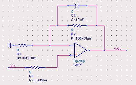
Until one day, I want to amplify a signal of 100kHz (good luck, frequency is not too high, otherwise the voltage feedback op amp can not play), also according to experience and a capacitor, and then. . . The signal is no longer normal. . . Because, this capacitive feedback impedance is reduced to less than 200Ω for a 100kHz signal, resulting in a change in the amplification factor.
Of course, this is not the key. The question is: Do you really need a compensation capacitor?
First, there is a pole inside the op amp (it thinks it is caused by RC low-pass), which causes a phase change, up to -90°:

If you add another pole, it will change the phase again, and the maximum can be increased to 90°:
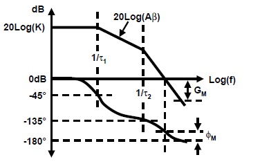
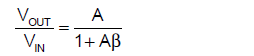
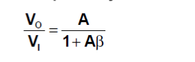
So the phase is -180°, what's the problem? That is the "shock." Take a look at the gain of the voltage negative feedback op amp:
When the loop gain Aβ at some frequency points is equal to 1 and the phase is -180°, then Vout/Vin will become infinite and the circuit will be unstable. Therefore, when a zero is added externally, the op amp will enter the oscillation at some frequency points , such as the distributed capacitance on the pin, as shown below:
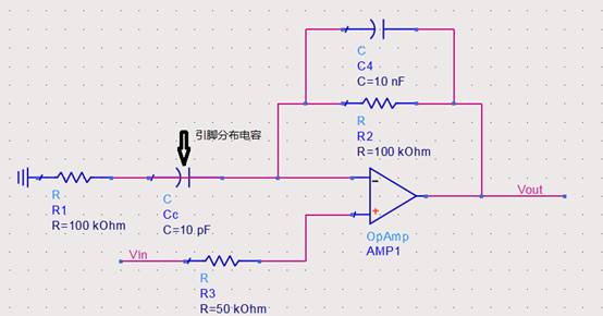
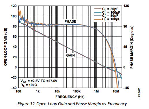
At this time, we put on a capacitor, which is equivalent to artificially introducing a zero point and pulling the pulled down phase . However, this distributed capacitance is generally small, so that its loop gain Aβ is equal to 1 and the position is very far. At the frequency, the op amp has not been working properly. Looking at the manual, the op amp itself is at 100k, the phase margin is quite high, exceeding 90°, and there is no need to add additional compensation capacitors.
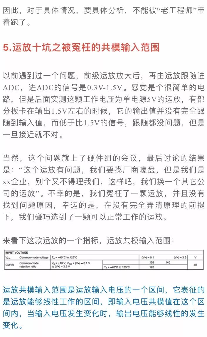
For the follower circuit, due to the negative feedback, the positive phase input terminal voltage and the negative phase input terminal voltage are basically the same value, and the common mode input range is -0.1V to the 5V power supply. 1.5V. Therefore, when the input voltage is around 1.5V, there is a case where the op amp cannot be linearly followed normally.
Why can't you follow? Let's look at a triode amplifier circuit, which is also part of the op amp, for illustration.
When the input Vb changes, Ie will change correspondingly with Vb, causing Vc to change, which is followed. If Vb continues to increase to Vc=Vcc-Ie x Rc, the calculated value is negative, but in fact Ie x Rc cannot exceed Vcc. At this time, the amplifying circuit reaches saturation or even the current is inverted, resulting in fixed or cut output voltage. Peak or reverse, etc.
6. The non-negligible slew rate of the ten-hole of the operational amplifier
To do a 1pps driver circuit, the rising edge is required to be ≤5ns. After the signal output from the FPGA is followed by the enhanced driver with the op amp, it is found that the rising edge does not meet the requirements. why? Because it does not take into account an important indicator, the slew rate. The slew rate is the average of the time-varying rate of the output voltage of the closed-loop amplifier when the input is a step signal. That is, input an ideal step signal, the output will be a signal with a slope, and the rate of climb of this signal is the slew rate.
Take a look at the slew rate of this op amp:
It can't meet the requirements at all. 5ns can only climb 20mV, so the rising edge can't meet the design requirements. How to do it? A pulse boost circuit has been added to the late fly line.
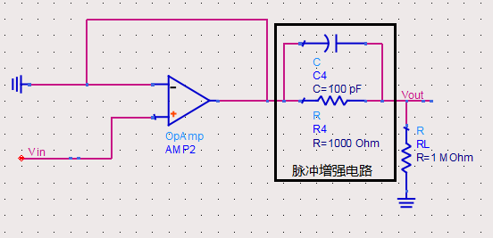
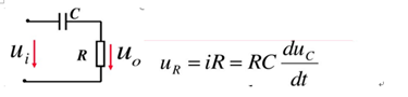
The pulse enhancement circuits C4 and R4, which correspond to a differentiating circuit C4 and RL (when C x RL is much smaller than the slew rate time) plus a DC resistor R4, make the signal edges on the load RL steeper. Analyze:
a. Capacitor C4 and RL form a voltage dividing circuit. According to the calculation formula of the following figure, the rate of change of voltage on C4 is equal to the voltage value on RL.
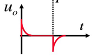
b. Then assume that the capacitance voltage change rate is almost unchanged in the range of 0-Ï„, then the voltage above the load RL is almost constant. Once the capacitor starts to charge (voltage changes), the voltage of the load RL rises to the top. . Recorded as waveform 1, as shown below.
c. Then start to fall after the capacitor is charged. In order to solve the problem that there is no voltage without change rate, add a DC resistor R4 to maintain the waveform. It is a through waveform, which is the original waveform, which is recorded as waveform 2.
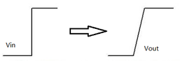
d. After the two waveforms are combined, the rising edge of waveform 2 is greatly enhanced due to waveform 1, so that the rising edge of the synthesized waveform is improved.
7. Forgotten feedback resistor of the ten-hole of the operational amplifier
In order to expand the external drive capability, a follower circuit is generally added at the last stage, and the current feedback op amp-CFA is selected to increase the output bandwidth of the op amp. It’s so simple, but unfortunately you can’t adjust it. Or look at the picture first. It’s so simple, but unfortunately you can’t adjust it. Or look at the picture first.
What power rail, common mode input range, gain product bandwidth, load capacity, slew rate. . . I have all considered it, or is it wrong?
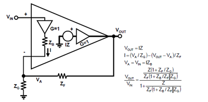
Because CFA and VFA (voltage feedback op amp) are not the same , the op amps that are used in reading, basically the teachers use VFA to give examples and explanations. The figure below is a model of the CFA op amp:
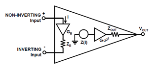
It differs from VFA in that the input is no longer both imaginary, the inverting input resistance Z B is a very small value, but it must not be considered zero; its open loop gain Gout is no longer very large, and It is approximately equal to 1; its transimpedance Z can be considered to be infinite.
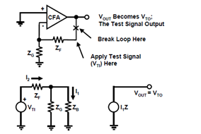
Therefore, the circuit model of the CFA follower circuit is as follows:
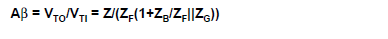
Solving Aβ is equal to:
Its closed loop gain is:
When there is no feedback resistor ZF, A is approximately equal to 1, ZF approaches 0, Aβ approaches infinity, and the gain approaches 0, which is completely different from the desired follower circuit, which is often referred to as “CFA not on the Internetâ€. There is no signal when adding a feedback resistor." (I didn't find this sentence, I forgot where I saw it. I can only see the introduction of feedback resistors in the CFA manual.)

Therefore, to add a feedback resistor, the circuit will work properly.
PS: The above derivation calculation is skillful and can only be derived from Aβ calculation, because the calculation premise of CFA is that the inverting input resistance Z B is a very small value; its transimpedance Z can be considered as infinite, so it is necessary to find the limit. Is to find a single variable, if you follow the final expression to find the limit, a function, three variables (Z F approaches 0, Z B approaches 0, Z approaches infinity), can't play, as shown below.
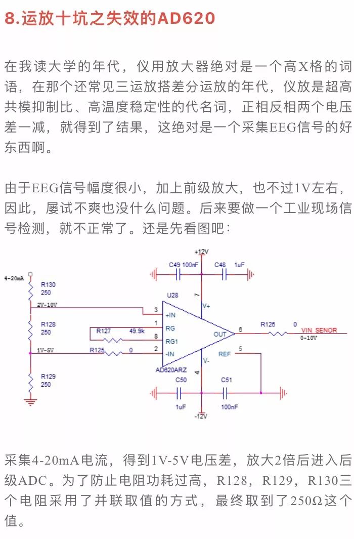
Analysis, the positive phase input terminal 2V-10V, in line with the device input range (VCC-1.4V), inverting input terminal 1V-5V, I added negative power, it is more consistent; then see the magnification factor 2 times, Vmax = 10V, also meets the device output range (VCC-1.4V); power supply, amplification, decoupling, etc. are no problem. This is a schematic that appears to have no errors, but in reality it will make an error at high input voltage values.
Look at the internal principle of the instrument, you will understand (here choose a hand on the information, not the internal principle of the AD620, in fact, the principle of the instrument is similar)
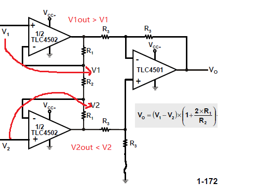
The positive phase input voltage and the inverting input voltage are reflected in the R2 inside the instrument, and the actual output voltage is reflected by V1out and V2out. In other words, the final added voltage value is divided into two parts, one by V1out provides, it will be higher than V1, and the other is provided by V2out, which will be lower than V2.
Looking at the schematic diagram, at 20 mA, Vin+ reaches 10V, Vin- is 5V, and is amplified by 2 times. In the instrument, it is necessary to enlarge Vin+ to 12.5V. This has exceeded the supply voltage of the instrument, so it is absolutely impossible to work properly.
9. The sampling time of the ADC of the op amp ten pit is dragged down by the op amp
The ADC collects signals, and when the signal is stable, it is very accurate; when the signal changes, the data is unstable. Of course, the ADC has sampling time, and the software engineer knows that he took 10 times and only took it 5 times, but the data is still unstable. Let the hardware look at the circuit. The hardware engineer said that the circuit is of course no problem. It is all deducted from others. How can I have problems with me?
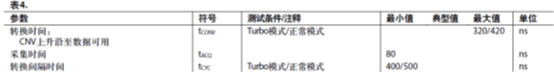
First look at the ADC's indicators Tcycmin = 500ns and Tacqmin = 80ns, this is a SAR ADC, the speed can be Mbps, fairly fast. Therefore, it is sampled 10 times in a row, and the time taken is only about 10 μs.
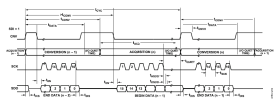
The op amp from the signal input to the output is not a process without delay, but a process with delay and oscillation. At the same time, the time of this process will increase due to the PCB design of the subsequent circuit. As shown below:
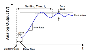
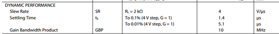
Look at the op amp's specifications. When 4V, it reaches 0.01%, the time is 5.1μs, and the fluctuation error is 0.4mV. In the 4V range, the 1LSB of a 16-bit ADC is 0.06mV. The error can eat 6, 7 code words. If the distributed capacitance and the trace resistance are added, this time will increase further, making the post-stage stabilization time increase, resulting in a larger error.

Later, the software engineer lowered the sampling rate, increased the acquisition time, and solved the problem.
10. The forgotten power consumption of the op amp ten pits
I have done a board and the power consumption is very strict. Therefore, after the design is completed, I draw a power tree and calculate the power consumption of each device. There is no super, then the board is commissioned, debugged, powered on, and the power consumption exceeds the standard. .
After a check, it was found that there was a problem in the calculation of the op amp power consumption. Five of the op amp circuits used in the figure below.
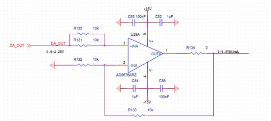
Because it is a DC drive, in the calculation, only the static power consumption of the op amp itself is considered, PD=15V x 4.2mA =63mW. According to the maximum static power consumption, the power consumption margin is more than enough.
In fact, an important power consumption point is neglected: the voltage difference between the op amp supply voltage of 15V and the output voltage (1V-4.5V) is all consumed in the op amp. According to the maximum differential voltage, one circuit consumes 140mW. This kind of dissipated power has never been considered before, so all of them are selectively ignored. When the demand for power consumption is tight, the problem is exposed.
Later, when the version was changed, the low voltage was selected to supply power to the op amp, which reduced the dissipated power consumption and met the requirements of the index.
A TPU Screen Protector made of the super toughness of the honeycomb structure. Its unique ultra-soft properties allow it to cover the most complex curves and contours in a device.
The self-healing design of the Hydrogel Screen Protector can protect the display screen of the device from damage, leave no air bubbles, and maintain the sensitivity of the touch screen. Advanced anti-fingerprint and dust- and oleophobic overlays keep your screen smudge- and dirt-free. This overlay is also important in providing maximum touch sensitivity for improved high-speed glide and optimal touch response.
The optical transparency of the Hydrogel Film is more than 90%, showing you the most original screen color and bringing the most realistic visual experience.
If you want to know more about the product information of the Hydrogel Screen Protector for iPhone, please click the product details to view the parameters, model, picture, price and other information of the iPhone Screen Protector.
Whether you are a group or an individual, we will do our best to provide you with accurate and comprehensive information about Hydrogel Screen Protectors!
Screen Protector For iPhone,Hydrogel Film for iPhone,Hydrogel Screen Protector For iPhone,TPU Screen Protector For iPhone,iPhone Screen Protector
Shenzhen Jianjiantong Technology Co., Ltd. , https://www.jjtscreenprotector.com