Summary
This paper explores a set of methods to solve the problem of power supply current failure in the chip unit level electrical test process. When a BiCMOS (Bipolar Complementary Metal Oxide Semiconductor) chip using QFN-MR (four-sided flat leadless-multiple-lead package) enters the mass production preparation period, power supply current failure is a manufacturing problem of advance and retreat.
This article describes several different failure analysis methods, such as data analysis, experimental design (DOE), flowchart analysis, statistical aided analysis, and benchmarking. These analytical methods are very helpful in determining the root cause of the problem, and then using statistics. Engineering tools gradually filter out the variables.
The project found the root cause of the current failure problem, and adopted corresponding solutions to reduce the incidence of power supply current failure, which is comparable to the main competitors. In the end, the project improved the overall yield of package testing by optimizing the company's internal resources without adding additional manufacturing costs.
These improvements also improve product quality and reduce the risk of customer complaints. After all the measures were put in place, the project saved manufacturing costs of 382,500 US dollars with the success of mass production.
1.0 PrefaceIn order to survive in the fast-changing semiconductor industry, whether it is internal users or external market customers, semiconductor manufacturers must establish a good image in the eyes of customers, which is the biggest semiconductor company to maintain market competitiveness and brand value. challenge. “Satisfaction†is a key element in building good customer relationships. On the contrary, business that cannot satisfy customers is unsustainable.
QFN-MR (four-sided flat leadless – multi-row lead package) is the largest product of the ST's Calamba plant and contributes a high percentage to the company's financial performance (according to global assessment criteria).
However, for the same customer to produce the same product, some outsourcing plants (outsourcing plant 1 and outsourcing plant 2) are superior in product quality, which forces the Kalamba plant to self-improve.
Product 1 is a QFN-MR product. In the preparatory stage of mass production, the total failure rate of the electric test power supply current is unqualified, and the total yield loss reaches 5.2%. Product 1 is a new product line at the Calma plant in STMicroelectronics. It needs to give the big customers an impression of fast delivery, but not at the expense of product quality. Therefore, it is necessary to find the main cause of product defects. In fact, solving these problems will give improvement opportunities to the Kalamba plant's mass production of similar product platforms.
1.1 Product 1 ConfigurationProduct 1 is a BiCMOS chip in a VPLGA package that controls the motor operation of the hard drive. Here VPLGA stands for ultra-thin grid array four-sided flat leadless – multi-row lead plastic package with a package thickness of 0.90 mm and 88 pins. Target applications include motor control for slim electronic devices and computer hard drives.
FIG. 1 is a schematic view of the package of the product 1.
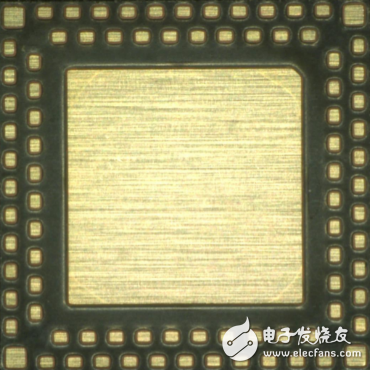
Figure 1: VPLGA88 Product Configuration / POD
1.2 BiCMOS Semiconductor Manufacturing Technology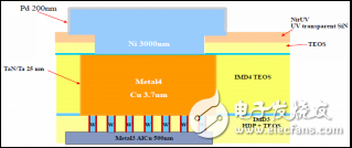
Figure 2: BiCMOS Semiconductor Manufacturing Technology
The BiCMOS chip consists of five layers. NiPd (nickel palladium) is the last metal layer on which the interconnect is placed.
1.3 QFN-MR Tapeless Lead Frame PackageThe tapeless four-sided flat leadless package is a lead frame package carrier (platform) that is post-etched to form a pin area on the carrier. Compared to other similar micro-packages, the tapeless QFN package brings better benefits to the ARM Calamba plant, for example, low lead frame cost, support for multiple rows of pins, compatible copper wire, tapeless carrier, wafer cutting high speed.
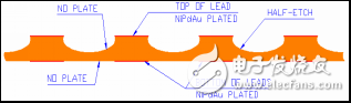
Figure 3: Tapeless QFN lead frame configuration
1.4 Product 1 test and all processes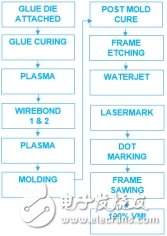
Figure 4: 1.4 Product 1 Packaging Process
Figure 4 shows the packaging process for Product 1, which was developed during the product development and certification testing phase, using the same chip manufacturing techniques and materials based on the existing packaging process.
1.5 Product 1 line stress performance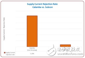
Figure 5: Comparison of power supply current rejection ratio
In the early stage of mass production of the product 1, the final test power supply current suppression ratio was 5.20%, far exceeding the outsourcing plant's 0.35%. The above bar chart is a comparison of the power supply current rejection ratio of the CANFA Calamba plant and the outsourced plant. The huge gap between the two places poses a major threat to the future business development of the ARM Calamba plant.
1.6 Benchmarking and Comparative AnalysisBenchmarking and comparative analysis were used to find out the difference in product manufacturing between the ARM-based Kalamba and the outsourcing plant. It should be noted that the outsourcing factory has a baking process after the waterjet process.
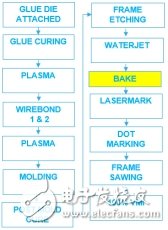
Figure 6: Comparison of manufacturing processes between STMicroelectronics and outsourced plants
At the beginning of the analysis, we found that the baking process was the main difference. After the wet process such as cleaning, a baking process is required to remove the moisture in the unit. Preliminary analysis showed that baking was the main factor in the final test of power supply current failure, and this huge discovery made the project team focus on the exploration of this process.
Similarly, the project team also made a micro-flow chart to determine the scope of the project.
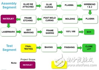
Figure 7: Microflow Chart Analysis / Package Flowchart
1.7 Description of the problemIn the mass production preparation period, the product 1 power supply current suppression ratio is 5.20%, which is classified as the moisture risk caused by the inherent wet process in the packaging process.
2.0 Experimental Section 2.1 Materials:§ Waterjet
§ QFN tapeless lead frame package
§ BiCMOS chip
§ Plastic unit
§ Inspection and test equipment
2.2 The experiment focuses on the main source, the waterjet process:It is important to determine the source of the problem and take corrective action. The research direction is mainly on the wet process. Based on the micro-flow chart analysis, the waterjet process is most likely to be the source of potential variation.
2.3 Dissection of the waterjet process:
In order to better understand the waterjet process, it is necessary to analyze the recording points step by step and observe the entire unit process from material preparation, loading and unloading to inspection.
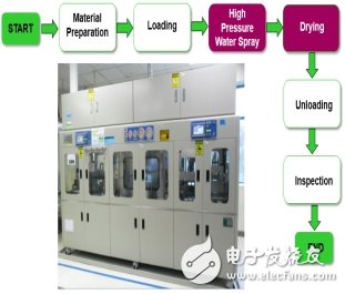
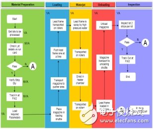
Figure 8: Detailed process of the waterjet process
2.4 Identify input changes:Use input and output methods to dig deeper into the changing factors. After intensive research, 42 KPIV variables were identified as important X factors, as shown in Figure 9. (See Appendix A for details)
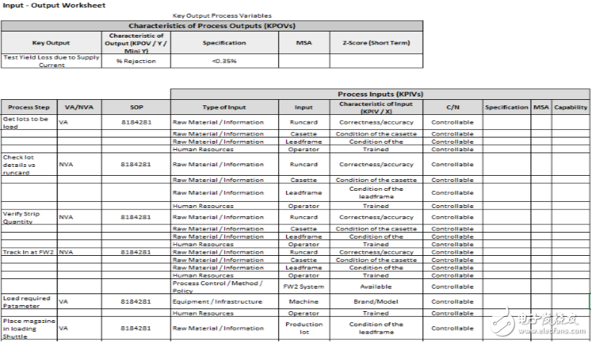
Figure 9: Input-Output Worksheet
2.5 Prioritize causality:The causal (C&E) matrix is ​​used to establish the internal relationship between the input variable and the X factor, as shown in Figure 10.
(See Appendix B for details)
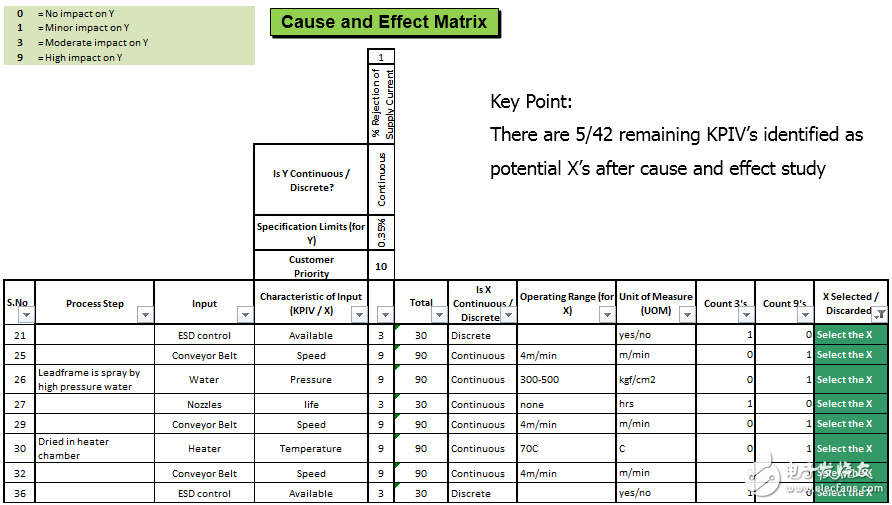
Figure 10: Causal Matrix
2.6 FMEA:The project team also used the FMEA failure mode and impact analysis to rethink the variable relationship. Since the supply current has no fault mode, consider all KPIV variables derived from the causal matrix, as shown in Figure 11. (See Appendix C for details)
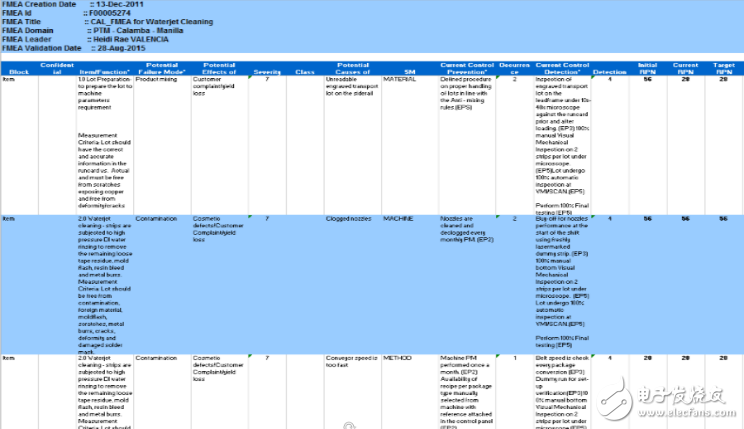
Figure 11: Failure Mode and Causal Matrix
2.7 Two quick-impact schemes:Upon completion of the above analysis, two (2) quick fixes were discovered immediately.
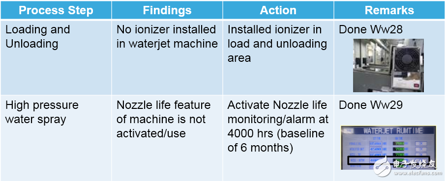
Figure 12: Temporary measure matrix
Analysis of results
A. Flow chart
· This project covers 18 process steps.
· 15 processes or 83% are VA (value added), 3 processes or 17% (no value added)
· No hidden factory found
· 42 potential X' factors were found in the input-output work order.
B. Causal matrix
· Find five potential X factors using a causal priority analysis.
C. FMEA
· Because the supply current is not initially identified as a failure mode, the five potential X factors are considered high risk.
D. Quick-impact scheme
· Found 2 quick-impact solutions
3.1 Verification scheme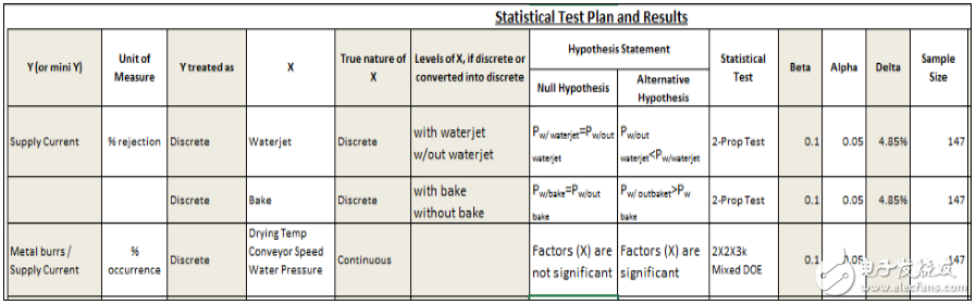
Figure 13: Verification scheme matrix
• Use the Proportional Test to verify two (2) items generated by GAP analysis (baking test)
• Verify three Xs using the mixed level DOE method.
(See Appendix D for details)
3.2 Statistical test
It is not difficult to find by observing the statistical hypothesis test results of Fig. 14 that the baking process behind the water jet affects the power supply current suppression ratio.
Practical conclusion: The power supply current suppression is lower in the waterless knife process, the R-square value is 22.78%, and the reliability is higher than 95%. If the waterjet process is not used, the supply current suppression is relatively low.
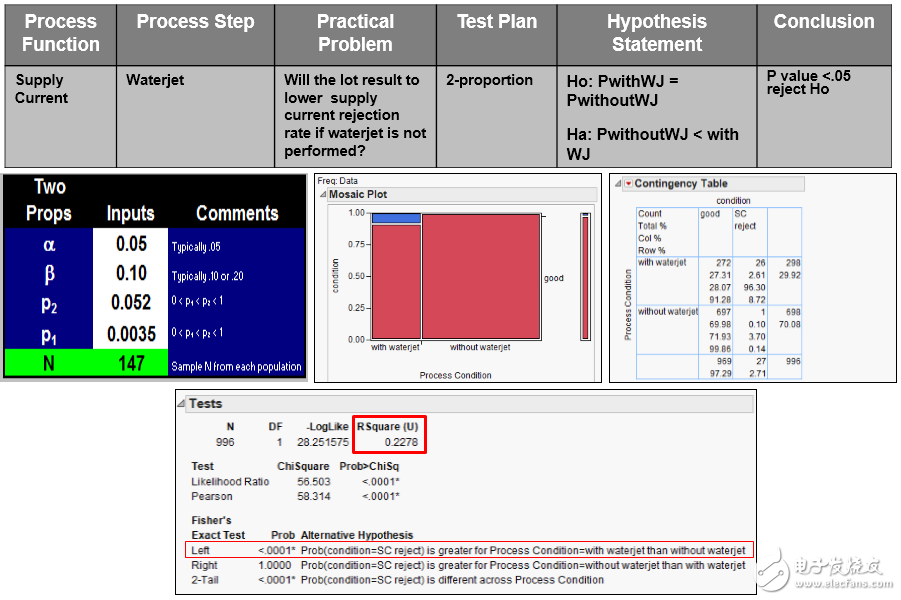
Figure 14: Hypothesis test
3.3 Verification scheme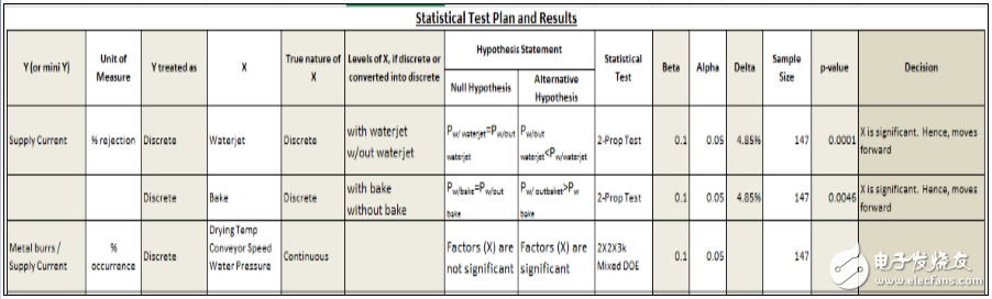
Figure 15: Verification results
The verification result (Fig. 15) shows that the power supply current suppression is affected by the grilling process behind the water jet. Therefore, if the waterless knife process is performed, the suppression ratio is lowered.
Based on key X factors that have been discovered, such as conveyor speed, baking temperature, and waterjet pressure, the project team used experimental design methods to further improve the waterjet process.
(See Appendix E for details)
3.4 Test Design (DOE)The test design method was used to analyze the conveyor belt speed, baking temperature and waterjet pressure parameters. The goal was to determine and set the optimal parameters to minimize the power supply current failure rate.
Figure 16 shows the experimental design for optimizing the critical parameters of the waterjet.

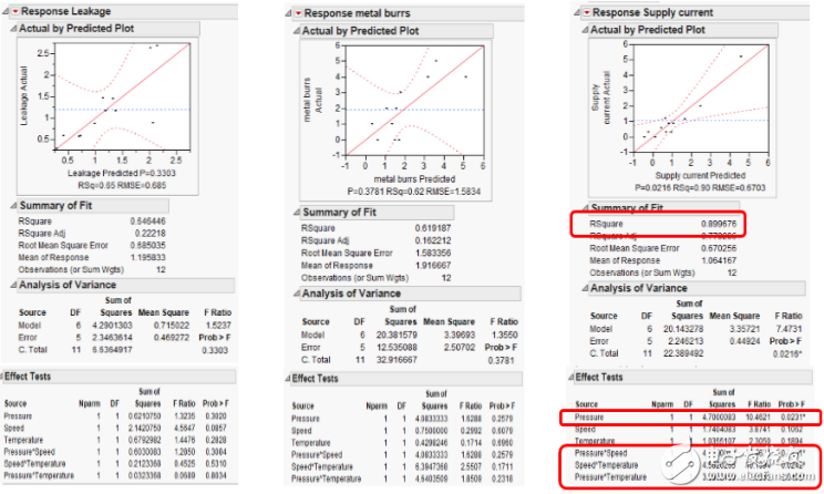
Figure 16: Experimental design and results
(See Appendix F for details)
From the experimental design results, when the P value is 0.0231, the pressure is the main factor affecting the power supply current suppression ratio. When the R-Square value is 0.8997, the pressure-velocity interaction (P value is 0.0231), the velocity-temperature interaction (P value is 0.0242), and the pressure-temperature interaction (P value 0.0405) is the influence of the power supply current suppression ratio. major factor.
According to the optimal setting given in the prediction profile of Figure 17, the maximum ideal parameters are obtained at pressure = 200 psi, speed = 3.5 m/min, temperature = 50 degC. Under these parameters, the power supply current rejection ratio is -0.238. +/- 1.156, the leakage is 0.414 +/- 1.84, and the metal burr is 1.338 +/- 4.63.
When P value = 0.0231, the pressure is the main factor affecting the power supply current failure; when P value = 0.0231, the interaction between pressure and speed is also the main factor; when P value = 0.0242, the interaction of speed and temperature is the main factor; When P value = 0.0405, the interaction between pressure and temperature is the main factor, and the reliability is higher than 95%.
Test statistics found that when the P value is 0.05, these main factors and interactions do not affect the leakage ratio and metal burrs.

Figure 17: Predictive Profiler Profile
It is not difficult to observe the predictive profiler report. When the pressure is 200 psi, the speed is 3.5 m/min, and the temperature is 50 degC, the power supply current suppression ratio, leakage and metal burrs are optimal.
3.5 Test Design (DOE) ConclusionWhen P value = 0.0231, the pressure is the main factor affecting the power supply current failure; when P value = 0.0231, the interaction between pressure and speed is also the main factor; when P value = 0.0242, the interaction of speed and temperature is the main factor; When P value = 0.0405, the interaction between pressure and temperature is the main factor, and the reliability is higher than 95%.
Test statistics found that when the P value is 0.05, these main factors and interactions do not affect leakage and metal burrs.
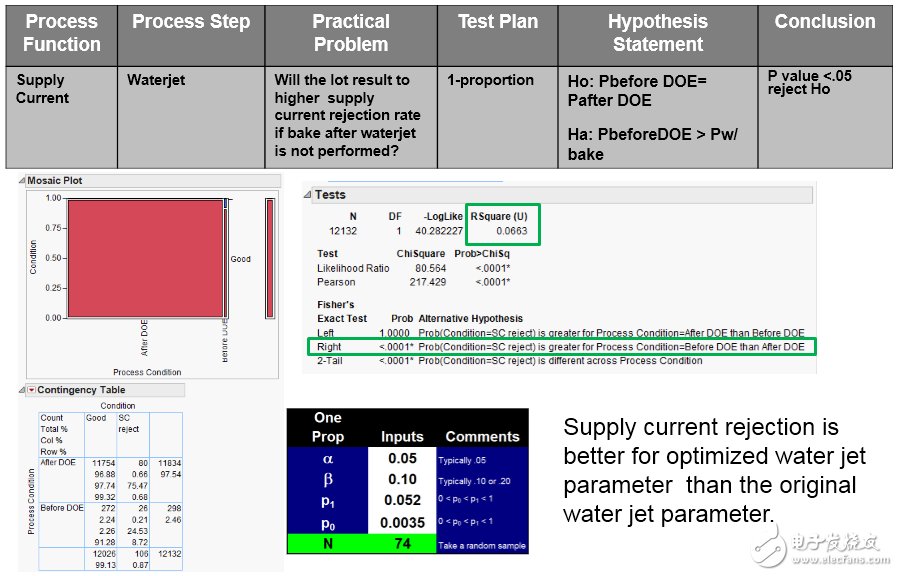
Figure 18: Results Verification Matrix
(See Appendix G for details)
3.6 How does the waterjet affect the product 1 power supply current failure?Understanding the knowledge of failure mechanisms can help improve the accuracy of statistical results:
• The frictional wear effect caused by the package permeability or high-speed water molecules increases as the waterjet pressure increases.
• High temperature blowers (same pressure) make gas molecules more kinetic and enhance friction and wear.
• The tape speed effect is most likely to affect frictional wear (contact speed), but is limited to the blower area, and the waterless environment gradually consumes the friction and wear effects.
3.7 Implementation resultsThe STMicroelectronics Kalanda plant achieved a 0.35% supply-to-current rejection ratio (outsourced plant benchmark), a significant improvement over the 5.2% pre-test.
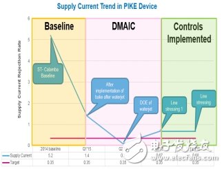
Figure 19: Power supply current rejection ratio trend analysis
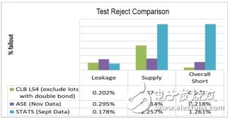
Figure 20: Comparison of the ST's Kalamba plant and outsourcing plant
to sum up:Leak
- The STMicroelectronics Kalamba plant (0.202%) is better than the outsourced plant 1 production batch (0.295%), and the outsourcing plant 2 is 0.178%.
Supply current
- The STMicroelectronics Kalamba plant (0.674%) is better than the outsourced plant 2 production batch (1.25%), and the outsourcing plant 1 is 0.314%.
b. Over-all short (SBL 0.5%)
- The STMicroelectronics Kalamba plant (0.071%) is better than the outsourced plant 1 production lot (0.218%) and the outsourced plant 2 1.261%.
3.8 Corrective measuresIn order to maintain the improvements achieved, the following measures need to be implemented and closely monitored:
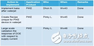
Figure 21: Correcting the preventive action matrix
3.9 DocumentationAll analytical activities and knowledge are documented for reference during product production. Control schemes, FMEAs, job instructions, and new processes including baking are documented.
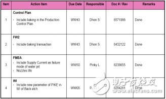
Figure 22: List of documentation
3.10 Promotion planIn order to make the most of the value of this R&D project, it is necessary to extend all the knowledge gained by the project team during the research process to other QFN-MR product manufacturing processes.

Figure 23: Promotion Table
3.11 Cost savingsAfter verifying the effectiveness of the corrective actions, the project team also estimated the cost savings of these measures.

Approved by IE at the Calma plant in STMicroelectronics, the total cost savings was $382.51 million.
4.0 ConclusionThis paper discusses the in-depth analysis statistical method to effectively solve the problem of power supply current failure in the final test process. Using statistical analysis knowledge and an understanding of data and defects can help you find the true root cause of defects. The comprehensive test design reduces the negative impact of the waterjet process on current failure. The introduction of the baking process significantly reduces the rate of current suppression ratio during the unit electrical test. The continuous failure rate reduction and the overall improvement of the product electrical test yield fully demonstrate the correctness and effectiveness of the verification corrective measures.
5.0 SuggestionsIt is recommended to implement approved corrective actions for a long time to stabilize the power supply current performance. The Six Sigma methodology (gradually dig deep into the problem, identify and validate the root cause of the problem, and achieve significant improvements under the premise of using existing resources without significantly increasing costs) is an effective means of solving manufacturing problems and should be promoted in solving similar problems. This method. Continuous benchmarking is also recommended, which helps companies improve their processes and rank among the best in the industry.
6.0 AcknowledgementThe authors would like to express their sincere gratitude to the following people: Jun Bernabe, Mariver Limosinero, Addonyz Antonio and all colleagues in the packaging department for their full support in this project.
Our family, friends, colleagues, colleagues, the success of this project is inseparable from their full support.
Special thanks to our Almighty God, always blessing our career development and living a happy life.
7.0 ReferencesIC Assembly handbook
2. BSA (Build Sheet Assembly)
3. SAS – JMP
4. Water jet Machine Manual
5. Package Portfolio & Technology Roadmap
8.0 About the author
Antonio 'Dhon' Sumagpang graduated from the Technical University of the Philippines (Manila Campus) with a bachelor's degree in electrical engineering (BSEE). He has 16 years of experience in the semiconductor industry and has extensive practical experience. After several years of working in different packaging processes at the ARM-based Calamba plant, the new product was introduced to a senior engineer and the new product was introduced to the project leader. The Best Technical Paper Award was awarded twice in the 20th and 25th ANTS (ASEMEP National Technical Seminar). Received numerous awards in the quality competition and holds the Green Belter certificate.

Francis Ann “Pinky†Llana graduated from St. LaSalle-Bacolod University with a Bachelor's degree in Chemical Engineering (BSChE) and has 18 years of experience in the semiconductor industry. He is currently a senior packaging engineer at the Kalamba plant of Arbitrary Semiconductor. Processes such as copper post-process etching, chemical stripping, bump design and electroplating have won numerous awards in regional and national quality competitions and hold the Green Belter certificate.

Ernani D. Padilla graduated from the Oriental University of the Philippines, a Chartered Electronic Communications Engineer and is a Senior Technical Engineer at the Kalamba Plant of Arbitrary France. He leads the Manufacturing Process Engineering team, specializing in injection molding and plasma processes, and holds Neville Clark's blackbelt certificate.
Type C Hub 8 In 1,Best Buy Usb C Hub,Usb C Hub For Macbook Pro,8 in 1 Type-C Multifunction Docking Station, 8 in 1 USB-C Multiport Docking Station
Shenzhen Konchang Electronic Technology Co.,Ltd , https://www.konchang.com