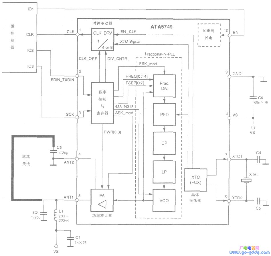
The ATA5749's power vs can use a single-cell lithium battery. As can be seen from the above figure, the ATA5749 is mainly composed of unit circuits such as PLL, digital control and register, clock driver, crystal oscillator (XTO) and power amplifier (PA).
1. The operation of the fractional N PLL PLL is controlled by a 32-bit configuration register. Using a 15-bit value frequency to determine the RF carrier frequency, RF carrier frequency software programming allows for certain multi-channel applications of the IC. The selected modulation type has a 1-bit ASK-NFSK flag, and FSK modulation is implemented by modifying the divider in the feedback loop. The 8-bit FSEP completes the FSK frequency offset from ±396 Hz to ±10 kHz at ±396 Hz per step. The PLL bandwidth is 140 to 380 kHz (typically 280 kHz), and the clock time of the PLL is 98.46 ms when using a 13.0000 MHz crystal.
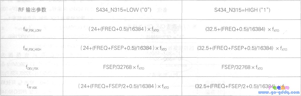
2. The RF carrier frequency selection fraction divider can be programmed according to the formula shown in the above table to generate an RF output frequency fRF. For fRFASK, if FSEP is an odd number, the FSEP/2 value should be rounded down to the next integer value. The FSEP can take values ​​from 1 to 255. When using a 1.300OOMHz crystal, the frequency offset fDEV_FSK range can be programmed from ±396Hz to ±101.16kHz per step ±396Hz. For example, when FSEP=100, the output frequency is FSK modulated, and at the crystal frequency fxro=1.30000 MHz, fDEV_FSK=±(FSEP/32768)×fXTO=±(100/32768)×1.30000 MHz=±39.6 kHz.
The frequency FREQ can range from 2500 to 22000. Using a 1.000000MHz crystal, by setting FREQ[0:14J=3730, FSEP[O:7]=100, S434_N315=0, the output fRF can be programmed to 315MHz; by setting FREQ[0:14]=14342, FSEP [0:7]=100, S434_N315=1, fRF can achieve 433.92MHz.
3. The power amplifier ATA5749's PA is a Class C amplifier with an open collector output delivering current pulses. The PA is enabled when the PLL is locked and the configuration register is programmed. The PA is enabled in the FSK mode and the RF output power is turned on. In ASK mode, the input signal must be set to high on the RF on the output pin. The output power of the PA can be programmed at approximately ldBm per step, ranging from -0.5dBm to +12.5dBm. The PA output current pulse peak lpulse can be programmed with a 4-bit value at power-on reset (PWR), allowing the user to scale the output power and current consumption to an optimum level.
4. Crystal Oscillator The ATA5749 crystal oscillator is a fixed-function amplitude-modulated precision oscillator that is enabled when EN is set. After the oscillator output amplitude reaches an acceptable level, XTO_RDY is set. If CLK_ON is set, pin CLK becomes active and the PLL receives its reference frequency. When using a small size crystal (such as 3.2mm x 2.5mm) with a 4fF dynamic capacitance CM, the crystal oscillator has a startup time of approximately 200μs. 5. The clock driver clock driver is programmed using the CLK_ONLY, CLK_ON, and DIV_CNTRL bits in the configuration register. When CLK_ONLY is cleared, normal operation is selected. When CLK_ONLY is set, the CLK output is enabled. When DIV_CNTRL is set, the clock divider can be set to divide by 4; when DIV_CNTRL is cleared, it can be set to divide by 8. When using a 1.300OOMHz crystal, an output of 3.25MHz or 1.625MHz will be produced. When CLK_ON is cleared, no clock is available on the CLK pin and the transmitter has a small current drain. The CLK signal is used to clock the microcontroller and can drive load capacitances up to 20pF and lOpF at 1.625MHz and 3.25MHz, respectively. The CLK outputs a low level when the IC is off and powered up. When the crystal oscillator amplitude detector detects sufficient amplitude and XTO_RDY and CLK_ON are asserted, the CLK output becomes active.
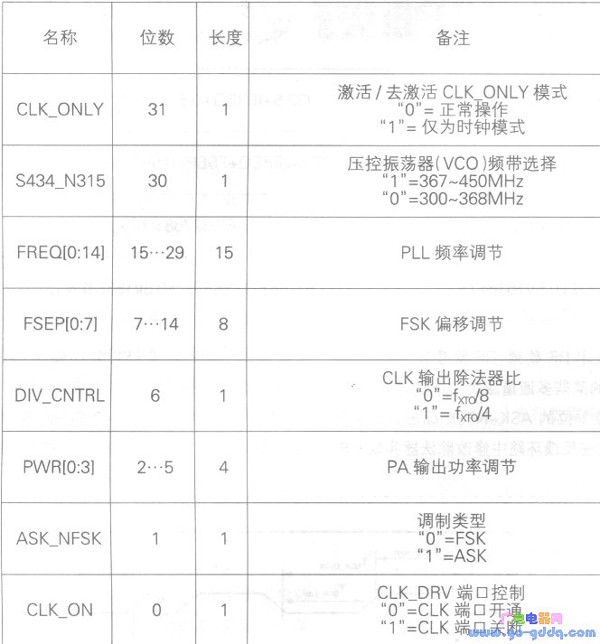
6. Configuration Registers and Their Programming When powering up or changing the operating parameters of the PLL transmitter, the user must program all 32 bits of the configuration register. The table below lists the bit assignments for the control registers.
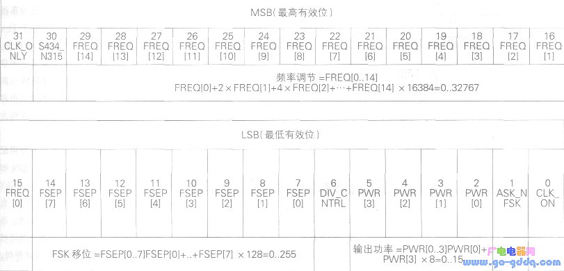
The functions of the control registers are shown in the table below.
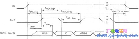
The configuration register is programmed from the MSB using the SPI bus. It consists of an enable line (EN), a data line (SDIN_TXDIN), and an SPI bus clock (SCK). The SDIN_TXDIN data is loaded on the SCK positive edge and the contents of the configuration register become the program on the negative SCK edge of the last bit (LSB) of the programming sequence. The figure below shows the timing diagram of the SPI bus. At the end of the 32-bit programming sequence, the SDIN_TXDIN line is the RF transmitter programming modulation input. After programming is complete, the SCK signal has no effect on the device. In order for the transmitter to go into shutdown mode, EN and SDIN_TXDIN must be returned to a low state.
After the configuration registers are programmed and RF data transmission is complete, the device enters shutdown mode and the crystal oscillator and PLL cease operation. The reset register mode can be used if the shutdown register mode is not entered and the configuration register contents are to be modified. To enter the reset register mode, SDIN_TXDIN must be held high while EN is low for the minimum reset time of at least 10μs.
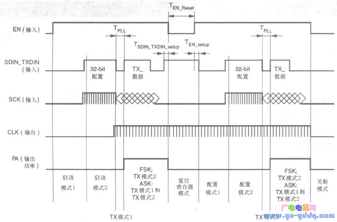
In the reset register mode, the PA and fractional PLL remain off, but the XTO remains active, which stays at 10 μs, followed by first raising EN and SDIN_TXDIN with a delay of 10 μs. In this mode, the 32-bit configuration register data is sent to the SPI bus. After the data is transmitted, the device is switched back to shutdown mode. In the meantime, EN, SCK, and SDIN_TXDIN must be kept low. The figure below shows an example of a programming timing diagram when using the reset register mode.
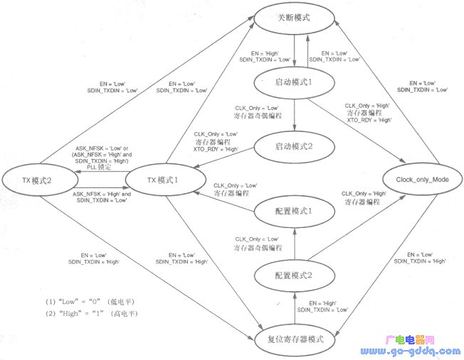
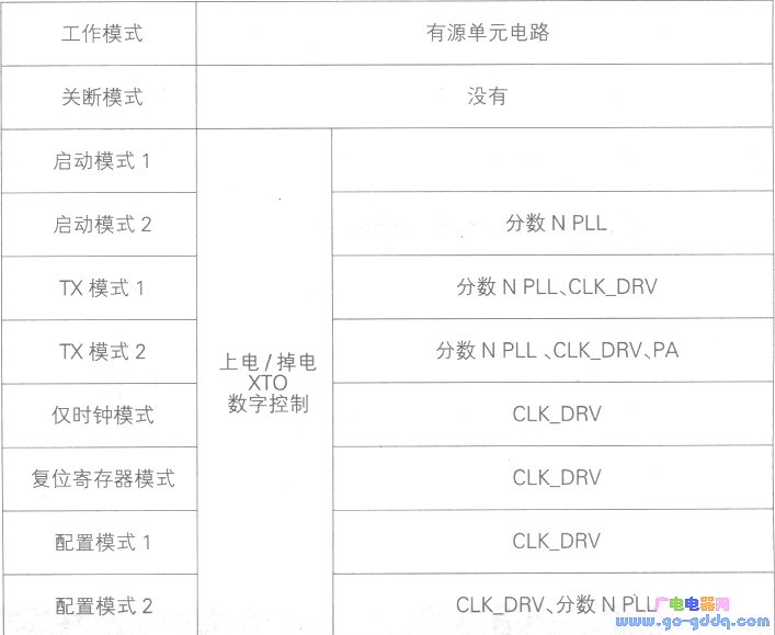
The figure below shows the operating mode status diagram of the ATA5749. In fact, the ATA5749 mode of operation is a function of the active circuit, as shown in the following table.
This website tries to open micro- and small-enterprise business advertising business; maintenance point recommended items. The fee is affordable and effective! Welcome to contact in QQ or email!
Why do you want to do online advertising contact?
- 0
- like
| Try to find the information you want to see. Inverter sensor patch three no weight loss camera LCD monitor does not boot digital camera XC9237 projector switching power supply laptop processor IPSUSB skills entrepreneurial black screen water heater can not boot circuit design silent transformer XC6102 without sound XC6112 display regulator no image microwave player successful silent GPS tea no picture XC6222 health XC6372 relay filter ML6209 switch washing machine digital camera description remote control without grating 555 protection circuit cancer self-closing Linux charger mobile phone shutdown noise inverter oscilloscope robot Windows antenna indicator light is not bright fiber life transformer stomach market alarm Hard disk watch embedded system woman maintenance process memory XC9236 converter router interview server kidney RFIDLED driver Konka CDMA instrument Panasonic CCD flashing engine multimeter Apple liver motor resistance keyboard integrated circuit current transformer triode governor power supply LED |
Plastic Package Diode.Among the electronic components, a device having two electrodes allows only the current to flow in a single direction, and many uses apply its rectification function. The Varicap Diode is used as an electronic adjustable capacitor. Most of the diodes have a current directionality that we often call the "Rectifying" function. The most common function of a diode is to allow only current to pass in a single direction (referred to as forward bias) and block in the reverse direction (referred to as reverse bias). Therefore, the diode can be thought of as an electronic version of the check valve.
Plastic Package Diode,High Frequency Diode,High Voltage Avalanche Diode,Plastic Package Zener Diode
YANGZHOU POSITIONING TECH CO., LTD. , https://www.cndingweitech.com