Author: Texas Instruments Emrys Maier, Tim Claycomb
Summary
Most Texas Instruments (TI) ultra-small outline leadless (X2SON) device circuit board layout and steel mesh information are provided in their data sheets. This document helps printed circuit board (PCB) designers understand and better use this information to optimize the design.
Due to the small package size of X2SON, the use of X2SON package allows users to compress PCB layout and realize the design of extremely small space. When using this space-saving package, understanding some key PCB manufacturing and assembly restrictions can reduce the complexity of the final product. This application report will discuss some limitations when manufacturing and assembling PCBs containing X2SON packages. There are three main factors that affect the package size and pitch of the printed circuit board (PCB). They are: PCB manufacturing, solder application and component layout.
introduction
Most Texas Instruments (TI) ultra-small outline leadless (X2SON) device circuit board layout and steel mesh information are provided in their data sheets. This document helps printed circuit board (PCB) designers understand and better use this information to optimize the design.
Due to the small package size of X2SON, the use of X2SON package allows users to compress PCB layout and realize the design of extremely small space. When using this space-saving package, understanding some key PCB manufacturing and assembly restrictions can reduce the complexity of the final product. This application report will discuss some limitations when manufacturing and assembling PCBs containing X2SON packages. There are three main factors that affect the package size and pitch of the printed circuit board (PCB). They are: PCB manufacturing, solder application and component layout.
2 PCB manufacturing
The design of the PCB must meet the manufacturing specifications of the PCB manufacturer. The manufacturability of the PCB depends on the required gap specifications. Tighter gap specifications will increase complexity and limit the number of available manufacturers.
Most mature printed circuit board manufacturers can produce copper layers with pitch and wiring of 0.1 mm (~4 mil) and can drill holes as small as 0.1 mm (~4 mil). The basic PCB size of the X2SON series package requires only 0.208 mm (8.2 mil) pitch-this is entirely within the manufacturing range.
The main problem in manufacturing with these packages comes from the method used to connect the center pins. The manufacturability of PCB will be affected by four main gap specifications: wiring pitch, wiring width, drilled hole diameter and ring diameter. Figure 3 visualizes each specification.
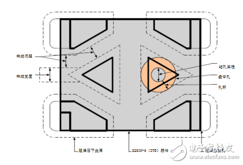
Figure 3. Gap specifications
Figure 4 shows the first option for connecting the center pin. This option is used for wiring between two pins of the same layer in the X2SON-5 (DPW) package. This will introduce wiring pitch and wiring width limitations. The maximum spacing between corner pads is 0.26 mm (10.2 mil), and it is assumed that the minimum wiring width allowed to be manufactured without increasing complexity is 0.1 mm (~4 mil), and the minimum wiring spacing is 0.08 mm (3.15 mil) ). Wiring spacing requirements less than 0.1 mm (~4 mil) will increase the complexity of manufacturing, some PCB manufacturers may not be able to manufacture. At the time of writing, major PCB manufacturers can achieve a detail accuracy of 0.05 mm (~2 mil).
Figure 5 shows the second option for routing to the center pin. This option is routed on a separate signal layer of the X2SON-5 (DPW) package pad and uses vias to connect to the center pin. By routing on the bottom layer, tight wiring pitch and wiring width on the top layer can be avoided. This layout method will lead to other limitations related to the size of the drill hole and the ring of holes. To avoid increased complexity and possible manufacturing problems, the drill hole diameter must be kept greater than 0.1 mm (~4 mil). In addition, the via diameter must be less than 0.35 mm (13.78 mil) so that the via is smaller than the center pin. This requires a minimum aperture ring specification of 0.125 mm (~5 mil). Because most PCB manufacturers can easily achieve 0.125 mm hole ring specifications, this option provides the most effective solution.
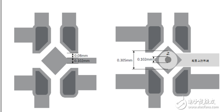
Figure 4. X2SON-5 (DPW) package center pin layout option 1 Figure 5. X2SON-5 (DPW) package center pin layout option 2
When setting through-holes on the center pad, the drill hole size restrictions must be considered. Use a drill hole with a diameter of 0.1 mm (~4 mil) or less to place the through hole directly in the center pad. Figure 7 shows a 0.1 mm through hole for scaling on the center pad. Please note that if this method is used, it is recommended to use a slightly larger solder hole diameter on the welded steel mesh, because some solder will be sucked into the through hole. Even if the solder is placed slightly outside the pad, as long as the pad is not in contact with any other pad or solder, it will be pulled onto the pad.
Figures 6 and 7 show examples of layouts covered with appropriate devices. Note that the solder mask window is larger than the external pads, which allows visual solder inspection of these pads. In addition, the pad metal extends under the solder mask to increase the physical strength of the pad. Accurate measurements are provided in the mechanical drawing section of each device data sheet.
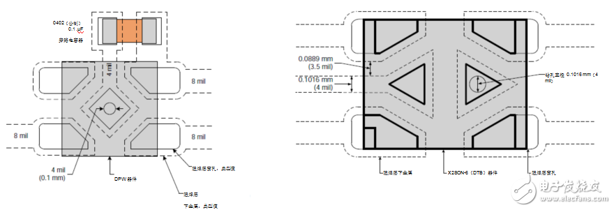
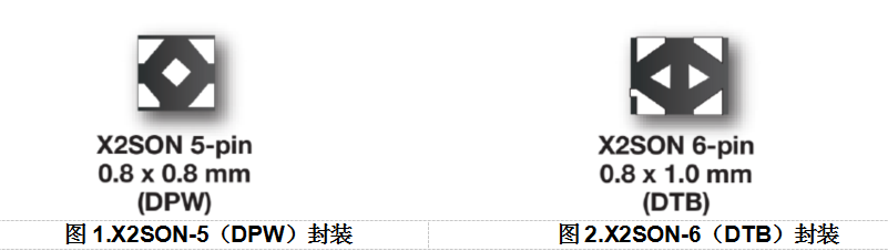
Figure 6. X2SON-5 (DPW) package PCB complete package example, showing bypass capacitors Figure 7. X2SON-6 (DTB) package PCB package example, not showing bypass capacitors
3 Application of solder paste
Due to the many issues involved, solder paste application is the most concerned area for small parts. The correct amount of solder needs to be placed on the pad. The amount of solder is affected by the thickness of the steel mesh, the type of solder, and the size and shape of the aperture. This becomes more difficult for packages with a pitch of less than 0.4 mm (15.7 mil). TI's X2SON package maintains a 0.4 mm (15.7 mil) pitch, while reducing the overall package size, so that more errors in the assembly process will not have a significant impact on yield.
TI recommends using a 0.1 mm (~4 mil) thick solder steel mesh with an aperture size between 92% and 100% of the pad size for proper solder deposition. When using the hole-in-disk method, this should be increased by 10%. Figures 8 and 9 show TI's solder paste recommendations for X2SON-5 (DPW) and X2SON-6 (DTB) packages, respectively.
The size of the solder steel mesh aperture is related to the selection of solder paste. Today, there are two main types of solder paste for SMT soldering: type III and type IV. Type III solder paste has now become the standard. When more consistent and finer particles are needed, type IV solder paste is used. Type III solder paste contains particles with a diameter of 25-45 μm (0.98-1.77 mil), and type IV solder contains particles with a diameter of 20-38 μm (0.79-1.50 mil). A typical rule of thumb is that the aperture width should be at least 5 times the size of the solder ball. Considering the 0.24 mm (9.45 mil) aperture shown in Figure 8, the solder ball diameter must be less than 0.048 mm (1.89 mil), which means that type III solder paste can be used.
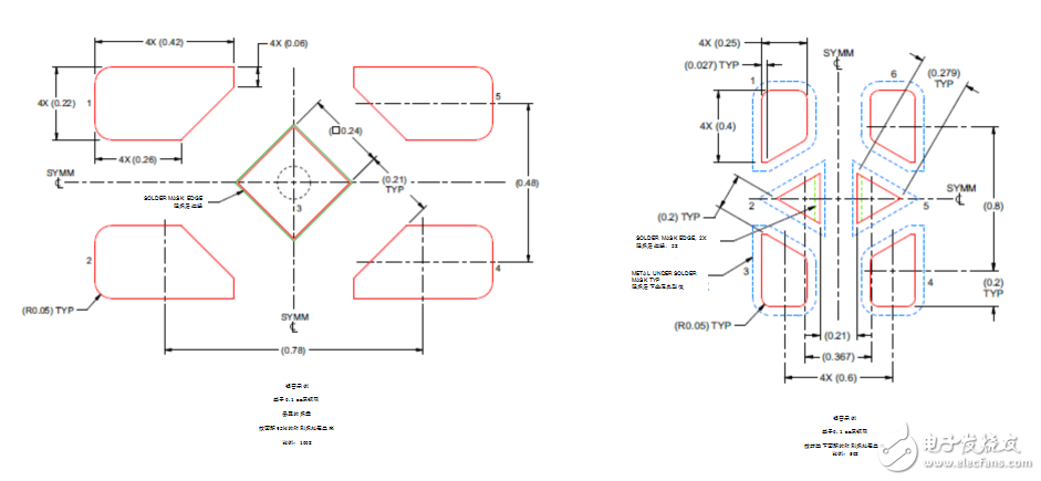
Figure 8. Example of X2SON-5 (DPW) package solder stencil Figure 9. Example of X2SON-6 (DTB) package solder stencil
Component layout
The placement of components for placement machines is usually very accurate, with an accuracy of about ±30μm. Figures 10 and 11 show that one-third of the pad layout of the X2SON package is incorrect. In order to install the components correctly, the X2SON-5 package requires an accuracy of ±83 μm (3.28 mil) or higher, while the X2SON-6 package requires an accuracy of ±72 μm (2.94 mil). This allows all pins to make good contact with the solder paste and prevents them from aligning with the pad by more than a third. During the soldering process, surface tension from the molten solder will align the parts. Since many placement machines are better than the required accuracy values, this issue should not be a problem for major PCB assembly companies.
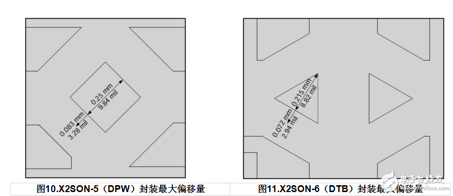
Figure 10. Maximum offset of X2SON-5 (DPW) package Figure 11. Maximum offset of X2SON-6 (DTB) package
LANA Vape is so convenient, portable, and small volume, you just need to take them out of your pocket and take a puff,
feel the cloud of smoke, and the fragrance of fruit surrounding you. It's so great.
We are China leading manufacturer and supplier of Disposable Vapes puff bars, lana bar vape, lana vape pod, lana vape pen,
lana disposable vape pen, and e-cigarette kit, and we specialize in disposable vapes, e-cigarette vape pens, e-cigarette kits, etc.
lana bar vape, lana vape pod, lana vape pen, lana disposable vape pen,lana disposable vape 2000 puffs
Ningbo Autrends International Trade Co.,Ltd. , https://www.mosvapor.com