MCUs can be divided into two categories according to the storage structure: one is the Harvard structure, and the other is the Princeton structure.
1 Harvard structure The so-called Harvard structure refers to the single-chip structure of the program memory address space and the data memory address space. For example, the 80C51 MCU adopts the Harvard structure, so the program memory address space of the 80C51 MCU is separated from the data memory address space, each has 64K storage. space.
2 Princeton structure The so-called Princeton structure refers to the combination of the program memory address space and the data memory address space. For example, the MCS-96 MCU uses the Princeton structure, so the program memory address space of the MCS-96 MCU and the data memory address space are merged. A total of 64K storage space.
1. SCM CPU
Figure 1 is a block diagram of the internal structure of the 80C51 microcontroller. If the memory circuit and I/O components in the figure are removed, the rest is the CPU. It can be divided into two parts: the operator and the controller. The arithmetic unit functions include an arithmetic logic unit ALU, an accumulator ACC, a register B, a temporary register TMP1, a TMP2, a program status word register PSW, and the like. The controller functions include a program counter PC, an instruction register IR, an instruction decoder ID, a timing control logic circuit CU, a data pointer register DPTR, a stack pointer SP, and a clock circuit.
(1) Operator
1 arithmetic logic unit ALU (Arithmetic Logical Unit)
The ALU can perform arithmetic and logic operations. Arithmetic operations include: addition, subtraction, multiplication, and division. The logical operations are: AND, OR, XOR, and so on.
2 accumulator ACC
The main function of the accumulator ACC is to store an operand before the operation, and store an operation result after the operation. Although the 80C51 series MCU still uses the accumulator A as an important component in the structure. However, due to the internal circuit taking measures, the core role of the accumulator A in data transmission, logic operation, etc. is weakened. Data can be transferred directly between the on-chip direct/indirect address memories without having to go through accumulator A. However, the operation results of the addition, subtraction, multiplication, and division arithmetic operations are stored in the accumulator A or AB register pair.
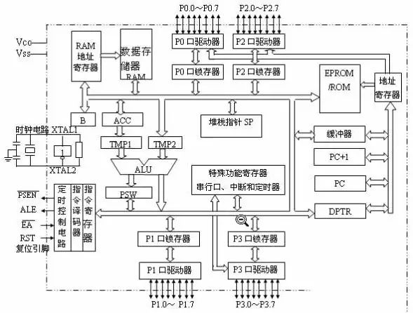
3 Registers TMP1, TMP2 As can be seen from Figure 1, the two operands before the ALU perform the arithmetic logic operation are from the registers TMP1 and TMP2, so the registers TMP1 and TMP2 are used to store the two operands before the operation.
4 program status word register PSW program status word register PSW is used to store the status flag of the operation result. The meanings of the PSW register bits are as follows, where PSW.1 is undefined, and the other descriptions are as follows:
| CY | AC | F0 | RS1 | RS0 | OV | / | P |
CY: Carry flag. It is the carry bit of accumulator A. It is set if the result of the operation has a carry (addition) or a borrow (subtraction) at the highest bit, otherwise cleared.
AC: Half carry flag. It is the lower nibble carry bit (the carry of the A3 bit to the A4 bit in accumulator A), mainly used for BCD code adjustment. When the lower 4 bits have a carry (when adding) or when there is a borrow to the upper 4 bits (when subtraction), AC is 1, otherwise, AC is cleared to 0.
F0: User-defined status flag. It can be set, reset or tested by software to control the flow of the program.
RS1, RS0: Working register area selection control bit, used to select one of the four sets of working registers. It can be set or cleared in software to determine the working register area. The correspondence between RS1, RS0 and register area is as follows:
RS1, RS0=00——0 area (address 00H~07H) RS1, RS0=01——1 area (address 08H~0FH) RS1, RS0=10——2 area (address 10H~17H) RS1, RS0=11 ——3 District (Address 18H~1FH)
OV: Overflow flag, used to indicate an overflow of signed arithmetic operations. OV is 1 when overflowing, otherwise OV is 0.
P: Parity flag. Each instruction cycle is set or cleared by hardware to indicate the parity of the number of 1s in accumulator A. If the number of 1 is an odd number, P is set; if the number of 1 is even, it is cleared.
5 register B
In the multiplication and division instruction, register B is used.
(2) Controller
The controller is a component that controls various operations of the microcontroller and is used to perform the operations specified by the instruction. It includes a program counter PC, an instruction register IR, an instruction decoder ID, a timing control logic, a data pointer register DPTR, a clock generator, a reset circuit, a stack pointer SP, and the like.
1 program counter PC
The program counter PC is a 16-bit register, which is used to store the next instruction address to be executed, and has an automatic 1 function.
2 instruction register IR, instruction decoder ID, timing control logic
The instruction register IR is used to temporarily store the currently fetched instruction, and is decoded by the instruction decoder ID to generate a corresponding decoding signal, which is sent to the timing control circuit, and the timing control circuit issues various control signals to control each device to complete the instruction. Operation.
3 data pointer DPTR
The DPTR is a 16-bit register. Since the 80C51 single-chip adopts the Harvard structure, its program memory is separated from the address memory. The address of the program memory is provided by the program counter PC, and the address of the data memory is provided by the data pointer DPTR, so the DPTR is used for storing off-chip. The address of the data memory and I/O port.
4 clock circuit
The clock circuit is the heart of the computer, which controls the working rhythm of the computer.
5 reset and reset circuit
The computer needs to be reset when it starts running. The reset is to make the CPU and other components in the system in a certain initial state and start working from this state.
6 stack pointer SP
The stack pointer SP is used to store the address of the top unit.
2. Memory configuration of the microcontroller
Since the 80C51 MCU adopts the Harvard structure, its program memory and data memory are separate, each with its own addressing system, control signals and functions. The program memory is used to store program and table constants; the data memory is usually used to store the given parameters and running results required for the program to run.
From the actual physical storage media, the 80C51 has four kinds of storage space, which are on-chip program memory, off-chip program memory, on-chip data memory (including special function registers) and off-chip data memory. The memory configuration of the 80C51 is shown in Figure 2.
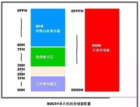
From the perspective of logical address space, the 80C51 microcontroller can be divided into three parts, namely: program memory, off-chip data memory, and on-chip data memory. These three parts use different address pointers and different access instructions. Therefore, the memory structure of the 80C51 is described below in a logical structure.
(1) Program memory
As can be seen from FIG. 3, the program memory uses the program counter PC as an address pointer, and through the 16-bit address bus, the addressable address space is 0000H~0FFFFH, which is 64K (216=64K) bytes, and the access instruction is MOVC. Used to store program instruction codes and fixed data tables.
The address space of the internal and external 64K bytes of program memory in the 80C51 microcontroller is uniform. For a microcontroller with internal ROM, in normal operation, the pin should be tied high to start the program from the internal ROM. When the PC value exceeds the capacity of the internal ROM, it will automatically move to the external program memory space.
(2) Off-chip data memory
As can be seen from the figure, the off-chip data memory uses DPTR as the address pointer. The 16-bit address bus has an addressable address space of 0000H~0FFFFH for a total of 64K (216=64K) bytes, and its access instruction is MOVX. Used to store data and operation results.
(3) On-chip memory
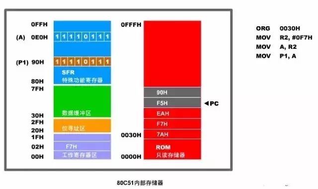
The address space of the on-chip data memory is 256 bytes from 00H to FFH, and the access instruction is MOV. Its address can be provided by the R0, R1 registers. The internal data memory is the most flexible address space. It is divided into two areas that are physically independent and different in nature: 128 bytes of RAM area composed of 00H~7FH units, special function register area with address of 80H~FFH (referred to as SFR area) ).
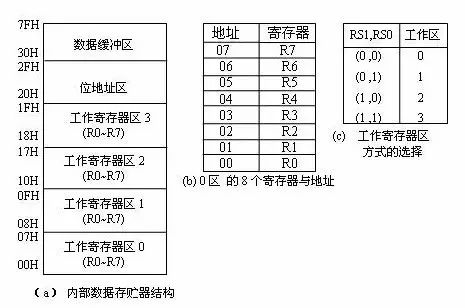
1) RAM area (00H~7FH)
As can be seen from Figure 2-3, the RAM area is further divided into three areas: a working register area, a bit address area, and a data buffer.
1 working register area (00H~1FH)
The internal RAM area structure of the 80C51 microcontroller is shown in Figure 2-3.
2-bit address area (20H~2FH)
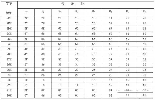
The internal RAM 20H~2FH is the bit addressing area, as shown in Table 1. Each of these 16 units has a bit address ranging from 00H to 7FH. Various program status flags and bit control variables are usually placed in the bit addressing area. The RAM area of ​​the bit addressing area can also be used as a general data buffer.
Table 1 Bit Address Map Table of Internal RAM Area
3 data buffer
The address space of the data buffer is 30 bytes from 30H~7FH, which is used to store data and operation results. For example, when adding, store addend, addend, and operation sum. Usually the stack area is also set in this area. Some microcontrollers set the display buffer in this area.
2) Special function register SFR (80H~FFH)
The I/O port latches, status flag registers, timers, serial ports, data buffers, and various control registers in the 80C51 microcontroller are collectively referred to as special function registers, which are discretely distributed in the internal RAM address space (80H~0FFH). Inside, Table 2 lists the identifiers, names, and addresses of these special function registers. It can be seen from Table 2-2 that the accumulator ACC, the register B, the program status word PSW, and the I/O ports P0 to P3 are all special function registers.
Table 2 Special Function Register SFR
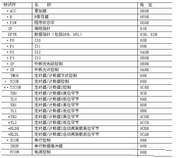
Note: Registers with the “·†sign can be addressed in byte and bitwise, which is characterized by a direct address divisible by 8. The register with the "*" sign is a register associated with Timer/Counter 2 and is only available in the 80C52 series. The following describes the internal memory of the microcontroller with an example.
3.80C51 single-chip parallel input/output port
The 80C51 microcontroller contains four 8-bit parallel I/O ports P0, P1, P2 and P3. Each port has 8 pins, as shown in Figure 2-1. There are 32 I/O pins, and each parallel I/O port can be used as an input or output. The first and second functions of each port are as follows:
I/O port pin first function second function P0 port P0.0~P0.7 input and output time-sharing transfer address lower 8 bits and data line P1 port P1.0~P0.7 input and output no second Function P2 port P2.0~P2.7 Input and output transfer address high 8-bit P3 port P3.0~P3.7 Input and output P3.0——RXD: serial port input
P3.1——TXD: Serial port output terminal P3.2——INT0: External interrupt 0 interrupt request input terminal P3.3——INT1: External interrupt 1 interrupt request input terminal P3.4——T0: Timer/ Counter 0 external input P3.5——T1: Timer/Counter 1 external input P3.6——WR: External data memory write strobe signal
P3.7——RD: External data memory read strobe signal
Each of the four channel ports has a special line structure, and each port contains a latch, namely special function registers P0~P3, one output driver and two (three in P3 ports) tristate buffers. This structure can be latched when the data is output, that is, the data on the port remains unchanged until the new data is re-outputted. However, the input signal is not latched, so the data to be input by the peripheral must be maintained until the fetch instruction is executed (after reading the data).
The structure, function, and usage of each port are described below.
(1) Composition and function of P0 port 1) Bit structure
When accessing the external memory, the P0 port is a true bidirectional data bus port, and the lower 8 bits of the address are sent out in time. Figure 2-4 shows a block diagram of the P0 port. It contains two input buffers, an output latch, and an output driver circuit and an output control circuit. The output drive circuit consists of two FETs V1 and V2 whose operating state is controlled by the output control circuit. The output control circuit includes an AND gate, an inverter, and a multi-channel analog switch MUX. Port 0 can be used both as a general purpose I/O port and as an address/data bus.
2) When the P0 port of the general-purpose I/O port is used as a general-purpose I/O port, the CPU causes the control signal to be low. At this time, the multi-way switch MUX turns on the end of the output latch of the B terminal, and simultaneously causes the AND gate to output a low level, and the FET V1 is turned off, so that the output stage is an open-drain output circuit.
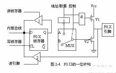
1 As the output port When the data is output by the P0 port, the write signal is applied to the clock terminal CL of the latch. At this time, the D terminal connected to the internal bus is inverted on the end of the data, and then reversed via the V2 tube. Phase, so the data appearing on the P0 port pin is exactly the data on the internal bus. Since the output stage is an open-drain circuit, an external pull-up resistor should be used as an output port.
2 as an input port When the P0 port is used to input data, one of the two three-state input buffers in the port is used. There are two ways to work: read pins and read latches.
When the CPU executes a general port input instruction, the "read pin" signal causes the next buffer in Figure 2-4 to be turned on, and the data on the port pin is then buffered into the internal bus.
When the CPU executes a "read-modify-write" instruction, the "read latch" signal causes a buffer on the top of Figure 2-4 to be turned on, and the data at the Q-side of the latch is input to the internal data bus via the buffer.
When the P0 port is used as an input port, "1" must first be written to the port latch. This is because if a read pin operation, if V2 is turned on, it will go low regardless of the input state on the pin. In order to properly read the logic level on the pin, first write a 1 to the latch, making its terminal 0 and V2 off. This pin becomes the high impedance input.
3) As the address/data bus port P0 can also be used as the address bus low 8 bits or data bus for system expansion. At this time, the control signal is at a high level, and the multiplexer MUX is turned on at the A terminal. There are two types of work: one is the bus output and the other is the external data input. As the bus output, the address or data signal input from the "address/data" terminal is driven by the AND gate to drive V2, and the non-gate is driven by V2, resulting in an address or data output signal on the pin.
When data is input as a data bus, external data input from the pin enters the internal data bus through the read pin buffer. For 80C51, 87C51 microcontrollers, the P0 port can be used as an I/O port or an address/data bus. For the 80C31 microcontroller, the P0 port can only be used as an address/data bus.
In summary, the P0 port can be used as an address/data bus port. At this time, it is a true bidirectional port, and can also be used as a general-purpose I/O port, but only a quasi-bidirectional port. The characteristics of the quasi-bidirectional port are: when reset, the port latch is set to "1", 8 pins can be used as a general input line, and when a pin changes from the original output state to the input state, it should be written first. Enter "1" to avoid misreading the information on the pin. Under normal circumstances, when the P0 port is used as an address/data bus port, it cannot be used as a general-purpose I/O port.
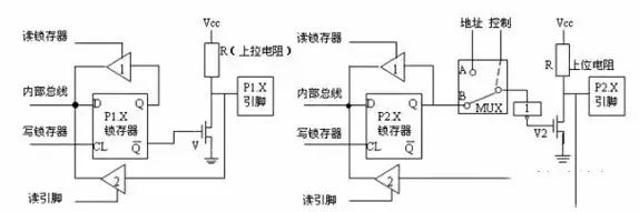
(2) P1 port composition and function
The P1 port is only used as a general-purpose I/O port, and its one-bit structure is shown in the figure. Compared with the P0 port, the bit structure diagram of the P1 port lacks the address/data transfer circuit and the multiplex switch, and the upper MOS transistor is changed to the pull-up resistor.
The function and usage of the P1 port as a general I/O is similar to that of the P0 port. When entering data, first write "1" to the port. It also has two ways of reading the pin and reading the latch. The difference is that when the data is output, since there is a pull-up resistor inside, there is no need to externally pull up the resistor.
(3) Composition and function of P2 port
When an external memory is connected to the system, the P2 port can be used to output a high 8-bit address. If it is used as a general-purpose I/O port, the P2 port is a quasi-bidirectional port. Therefore, the P2 port can be used as a general-purpose I/O port or an address bus, and its one-bit structure is as shown.
1 as a general purpose I / O port
When the control signal is low, the multiplexer is connected to the B terminal, and the P2 port is used as the general I/O port. Its function and usage are the same as those of the P1 port.
2 As the address bus When the control terminal outputs a high level, the multiplexer is connected to the A terminal, and the address signal is output through the inverter and the V slave pin. At this time, the P2 port output address bus is 8 bits high for system expansion.
For 80C51, 87C51 single-chip microcomputer, P2 port can be used as I/O port or address bus. For the 80C31 microcontroller, the P2 port can only be used as an address bus.
(4) P3 port composition and function
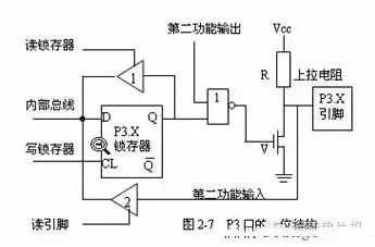
The P3 port can be used as a general-purpose I/O port, and each pin has a second function. One structure of the P3 port is shown in Figure 2-7.
As a general-purpose I/O port: When the "second function output" terminal is high, the P3 port is used as a general-purpose I/O port. At this time, the NAND gate is equivalent to the non-gate for the input terminal Q, and the bit structure is completely the same as the P2 port. Therefore, the function and the usage method when the P3 port is used as the general-purpose I/O port is the same as the P2 port and the P1 port.
Used as the second function: When a bit of the P3 port is used as the second function output, the latch of the bit should be set to "1", so that the output state of the NAND gate is only affected by the "second function output" side. control. The state of the "second function output" terminal is output to the bit pin via the NAND gate and the drive transistor V.
When a bit of the P3 port is used as the second function input, the latch of the bit and the "second function output" terminal should be "1", so that the input signal on the bit pin is sent through the buffer. Enter the "second function input" end.
At this point, the division of labor for each parallel port that constitutes a general-purpose microcontroller application system can be summarized as follows: P0 port: Time-sharing is used as the address lower 8 bits and data line, and the lower 8-bit address is provided by the PC lower 8 bits or DPL. P1 port: Bit-addressable input and output port. Port 2: The upper 8 bits of the address line, the upper 8 bits are provided by the PC's upper 8 bits or DPH. P3 port: Dual function port, if you do not use the second function, it can be used as a general I/O port.
Ms001 3000Puffs Vape,Mini Electronic Cigarette,Vape Electric Cigarette,Electronic Cigarette Vape Puff Bar
Guangzhou Yunge Tianhong Electronic Technology Co., Ltd , https://www.e-cigaretteyfactory.com