Current sampling circuit design
In this paper, a set of analog grid-connected power generation system is developed, which realizes functions such as frequency tracking, maximum power tracking, phase tracking, input undervoltage protection, output overcurrent protection, anti-islanding effect, etc. The internal integration timing is realized by Atmega16 high-speed single-chip microcomputer. Counter function; use the fast PWM function of timer T/C2 to realize the generation of SPWM signal; use T/C1 input capture function to realize frequency phase monitoring and tracking and detection of physical quantities such as distortion, input voltage and output current With control.
1 The overall scheme design adopts Atmega16 single-chip microcomputer as the main control circuit. The working process is as follows: the same frequency and same-phase sine wave as the reference signal is SPWM modulated, and then output sine wave pulse width modulation signal, which is driven to amplify and drive H bridge power. The tube works through a filter and a power frequency transformer to generate a sinusoidal current with a reference signal pass frequency and the same phase. Among them, overcurrent and undervoltage protection are realized by hardware, and functions such as synchronization signal acquisition, frequency acquisition, and control signal output are all completed by Atmega16. The overall design block diagram of the system is shown in Figure 1.
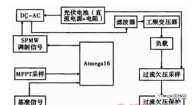
Figure 1: System pivot diagram
2 The hardware circuit design is divided into DC/AC drive circuit, DC/AC circuit and filter circuit 3 parts and smoothing capacitor C1. The circuit principle is shown in Figure 2.
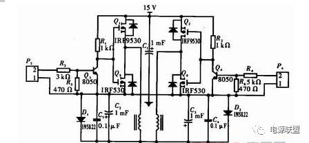
Figure 2: AC\DC converter circuit
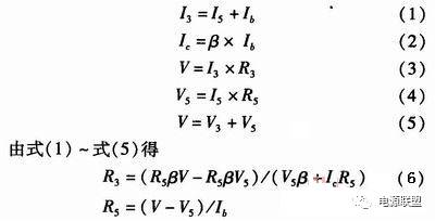
It is composed of R1, R2, R3, R4, R5, R6, Q3, Q4, P3 and P4, wherein P3 and P4 are control signal input terminals, and R3 and R4 are current limiting resistors. The current of the collector directly affects the steepness of the rising edge of the waveform, and the larger the collector current, the steeper the waveform of the output. Because R2 and R1 form a time constant of RC charge and discharge with the parasitic capacitance of the collector pn junction, the parasitic capacitance of the collector pn junction cannot be changed. Only by changing the values ​​of R1 and R2 to change the time constant, so R1 and R2 values The smaller the collector current of Q3 and Q4 is, the smaller the charging time constant of RC is, the steeper the rising edge of the waveform is, and the increase of collector current will increase the power consumption of the system, and the trade-off will choose a suitable value. Second, the parasitic capacitance of the emitter pn junction also affects the turn-off time of Q3 and Q4 and the steepness of the rising edge of the waveform. Therefore, a discharge circuit is added to the driving circuit, that is, the grounding resistors R5 and R6, the introduction of R5 and R6, accelerate the closing speed of Q3 and Q4, which makes the waveform of the collector steeper. Also, under the condition that the base emitter pn is not damaged, the current of the base is also larger as possible, but it also brings the loss problem, and the trade-offs choose a suitable value. Regarding the values ​​of the two resistors, it is assumed here that the amplification factor of the triode is β, the base current Ib, the collector current Ic, the current flowing through R5 is I5, the current flowing through R3 is I3, and the voltage drop of R3 is V3. The drive signal is V, and the voltage drop of R5 is V5.
In practice, R3 and R5 should be smaller than the calculated value. This is to make the triode work in saturation and improve system stability.
2.2 The DC-AC circuit is composed of two p-channel MOSFETs. Q1, Q2 and two n-channel MOSFETs Q5, Q6. There are no four n-channel MOSFETs used here. The reason is that the driving circuit is complicated. If the above two driving tubes are used, the two conductor tubes that are close to the power supply cannot be fully turned on, and the heat generation is more than 4 times that of the ground side conductor. Increased, so the use of the tube inverter reduces the power consumption, and the drive circuit is simple. The DC/AC function can be achieved by controlling the switching speed of the four conductor tubes and then passing through a low-pass filter.
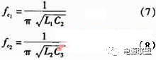
2.3 Filter circuit Two Schottky rectifier diodes 1N5822 are freewheeling diodes. Here, to prevent the generation of negative voltage, C2, C3, C4, C5, L1, L2 form a low-pass filter, where C5 and C6 are ceramic capacitors. , C2, C3 with electrolytic capacitors, charge and discharge current can flow into the ground, L1, L2 is the inductor with iron core, the inductance of the core with the high frequency is better than the hollow inductor, the inductance value is higher. The selection of parameters and the calculation of the cutoff frequency are as follows
3.1 Current sampling circuit design Because the terminal load is fixed, the current sampling is actually equivalent to a peak detection process. This circuit is actually a peak detection circuit. P3 is the two input terminals of the signal, and R10, R11 and R17 are adjusted. R18 takes the value to achieve the peak measurement function. The resistance value in the circuit is not accurate. It is necessary to adjust the resistance values ​​and ratios of R10, R11 and R17, R18 according to the amplitude of the signal. The current of R14, R15, R19 and R20 is more than 10 times of the internal bias current of the analog comparator. The resistance of the resistor is as large as possible, which reduces the power consumption and ensures the stability of the system. Y3 uses the analog comparator LM393. The LM393 has an internal collector output. When applied, the output terminal should be connected to a pull-up resistor. The circuit is shown in Figure 3.
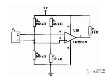
Figure 3: Current sampling circuit
3.2 MPPT Sampling Circuit In photovoltaic systems, it is usually required that the output power of the solar cell is always the largest, and the system should be able to track the maximum power point of the solar cell output. If the load does not work at the maximum power point provided by the battery, the maximum power that the battery can provide under current conditions cannot be fully utilized. Therefore, an impedance transformer must be added between the solar cell and the load so that the transformed operating point coincides with the maximum power point of the solar cell, so that the solar cell outputs at maximum power, which is the maximum power tracking of the solar cell. That is, the maximum power tracking MPPT is an important direction for the research of this set of photovoltaic grid-connected power generation simulation devices. Since the maximum power output point of a photovoltaic cell varies with light intensity, load, and temperature. To take full advantage of solar energy, the system must achieve maximum power point tracking. This set of photovoltaic grid-connected power generation simulation uses a constant voltage control method, which has the advantage of being simple and easy to track and can track the maximum power point. The working principle of the circuit: the core of the module circuit is also the analog comparator LM393, TL431 provides a reference voltage of 7.5 V, where the reference voltage value is recommended ≥ 7.5 V, the value can be slightly larger than 7.5 V, In order to improve the stability of the system, it should be ensured that the current flowing through R3 and R9 is more than 10 times of the bias current of the analog comparator LM393, and the values ​​of R3 and R9 are as large as possible. The parallel connection of R1 and R2 is convenient for debugging. In reality, it is difficult to find a resistor with a suitable resistance value. The sliding rheostat is expensive, so the parallel debugging effect with two resistors is ideal. Suppose R is a parallel value of R1 and R2, and the current flowing through R is I, then there is
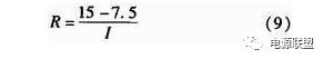
In equation (9), it can be considered as the minimum value of the sink current of TL431, and the current flowing through R6 and the bias current of analog comparator LM393 are ignored. For R6 and R13 resistance values, refer to the bias current of pin 1 of TL431. The current flowing through R6 and R13 should be 10 times the bias current of pin 1 of TL431, and the power consumption should be reduced as much as possible to ensure system stability. .
The output uses the optocoupler U4 to isolate the control circuit from the main circuit to prevent the main circuit from interfering with the control circuit. The values ​​of R4 and R5 are too large to affect the stability. If the value is too small, the current flowing through R4 and R5 is large. Add or even damage the device.
The analog comparator LM393 has a fixed voltage of 7.5 V at the positive input terminal 3, and a high level is acquired in PD4 under normal conditions. When the voltage at pin 2 is higher than 7.5 V, the output pin at the output pin is low. Ping, the optocoupler is turned on, and the PD4 collects a low level to start processing the SPWM signal to adjust the output impedance to achieve constant voltage tracking, and finally achieve maximum power point tracking. The circuit is shown in Figure 4.
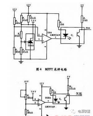
3.3 Undervoltage sampling circuit design As shown in Figure 5 and Figure 4, the inverting input of the analog comparator is 7.5 V reference voltage, and R22 is replaced by potentiometer. The purpose is to make the device suitable for adjustment. Different undervoltage control. The output uses optocoupler U4 to isolate the control circuit from the main circuit to prevent the main circuit from interfering with the control circuit. The values ​​of R22 and R24 are too large to affect the stability. If the value is too small, the current flowing through R22 and R24 will increase. Even if the device is damaged, the value of R21 and R23 can be found in the input and output characteristic curve of 4N25.
The inverting input terminal of analog comparator LM393 has a fixed voltage of 7.5 V. Under normal state, the undervoltage sampling output is high. When the voltage of pin 5 is <7.5 V, the output of pin 7 of the output terminal is low. Ping, the optocoupler is turned on, and the low-level undervoltage protection circuit collected by the undervoltage output starts to work, and the main circuit power supply is cut off to realize undervoltage protection.
4 Undervoltage and overcurrent protection circuit design circuit is shown in Figure 6. When the system works normally, the overcurrent protection signal and undervoltage of the overcurrent protection input are the 1st and 2nd feet of CD4011, and the detected signals are high. Level, C04011 3 pin output low level, after U10B and U10C two-stage inversion finally CD4011 10 pin output low level, triode 2N3904 cut off, relay normally closed end is in conduction state, the system is in normal working state. When the output current flowing through the load is too large or the input voltage is insufficient, the low level triggers the 1 pin 2 of the CD4011. At this time, the 3 pin outputs a high level, and the capacitor C10 is charged after the U10B and U10C are inverted in two stages. Level, the transistor 2N3904 is turned on, the normally closed end of the relay is disconnected, the main circuit stops supplying power, and is in a protection state. Since the main circuit power supply is cut off, the input of U10A detects a high level, and the 3 pin outputs a low level. Due to the high input impedance of CD4011 and the single-conduction of switching diode D6, the charge of C10 can only be released through R27, when U10B The input terminal potential is lower than the threshold voltage. After two stages of U10B and U10C are inverted, the transistor 2N3904 is turned off, and the main circuit starts to supply power. In this way, after the system over-current and under-voltage faults are eliminated, the device automatically returns to the normal state.
This part of the circuit is designed with dual input quad NAND gate CD4011 as inverter, switching diode D6, resistor R27, electrolytic capacitor C10, transistor 2N3904 and relay. The selection of R26 is determined by the drive current of the relay and the amplification factor β of 2N3904. If it is too small, the power consumption will increase, and if it is too large, the relay cannot be driven. The discharge time of R27 and C10 is the interval between the detection of the system undercurrent and undervoltage protection. Time T = 2 × R27 × C10.
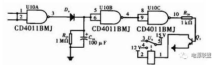
Figure 6: Undervoltage and overcurrent protection circuit design
Precision machining is a kind of machining, which is a workpiece to meet the requirements of the drawing of the line tolerance of the processing process, the workpiece in this process, will have certain changes in their performance characteristics and shape structure.
There are mechanical processing, naturally there are corresponding parts, mechanical parts design as a mechanical major of a subject, is one of the popular majors of science students, is also one of the strongest engineering; At present, this major requires not only good knowledge of science and engineering, but also excellent drawing ability and spatial imagination ability. In addition, due to the development of domestic industry and the constant change of demand, the demand for personnel in the mechanical processing industry is also increasing, and the employment rate of mechanical majors can reach 95%.
Precision Machining,Casting Exhaust Manifold,Stainless Stee Milling,Custom Cnc Machining Part
Tianhui Machine Co.,Ltd , https://www.thcastings.com