A switching converter is a main circuit that converts a power supply form into another form by using a semiconductor power device as a switch. The flyback switching power supply is a type of switching converter, and its main circuit is shown in FIG. Since the transformer has the same name on one side, the output voltage is negative and positive. When the driving signal is high level, the switch tube is turned on, the voltage source charges the primary side inductor, and the inductor current rises linearly until the switch tube is turned off, and the primary side current reaches a maximum value. During the conduction of the switch, since the diode is subjected to the reverse voltage, no current flows through the secondary side. When the drive signal is low, the switch is turned off, and the secondary diode is subjected to the forward voltage and begins to conduct.
The capacitor is charged while the capacitor is discharged through the resistor. The capacitor voltage is positive and negative.
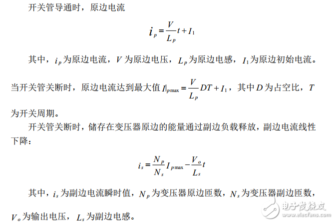
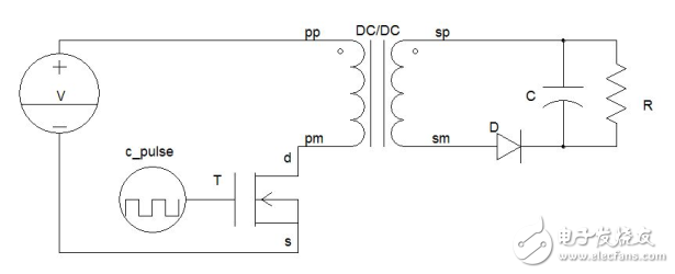
Figure 1 flyback circuit schematic
Flyback converters have two modes of operation, one for continuous operation and one for discontinuous operation. Before the drive signal of the next cycle comes, the current in the secondary side of the transformer has been reduced to zero. This mode of operation becomes the current discontinuous mode of operation. If the current in the secondary side of the transformer does not decrease to zero before the drive signal of the next cycle comes, this mode of operation becomes the current interrupt mode. Between continuous mode and discontinuous mode is a critical mode. In this state, when the next cycle signal comes, the inductor current is just reduced to 0. In order to avoid transformer core saturation, the transformer is usually designed to operate in a discontinuous mode.
The flyback converter has the following main features:
(1) The same name end of the primary winding of the high frequency transformer is opposite to the polarity of the same name of the secondary winding. The non-identical end of the primary winding and the driving end of the switching tube are common, and the same name of the primary winding is terminated with the positive terminal of the voltage source.
(2) The high-frequency transformer is equivalent to a storage inductor. When the switch is turned on, the transformer stores energy. When the switch is turned off, the energy is transmitted to the secondary side.
(3) It can work in continuous mode or discontinuous mode.
(4) An inverter that can constitute a DC input terminal, or an AC/DC converter that constitutes an AC input.
(5) The output voltage is lower or higher than the input voltage depending on the turns ratio of the high frequency transformer.
(6) Multiple outputs can be obtained by adding secondary windings and related circuits.
(7) Flyback converters generally do not require a low frequency filter inductor in series between the output rectifier diode and the filter capacitor.
2, UC3842 worksUC3842 is a high-performance, single-ended output, frequency-adjustable current-mode PWM modulator. The biggest advantage is that it has fewer external components, simple peripheral lines, and low price. It is widely used in switching power supplies in industrial products.
The main features of UC3842 are: 1 the frequency control of the oscillator is more accurate and can be fine-tuned; 2 the current working mode frequency can reach 500KHz; 3 automatic feedforward compensation function; 4 blocking PWM, cycle-by-cycle current limit; 5 built-in reference source, undervoltage Locked; 6 large current totem pole output, up to 1A; 7 undervoltage lockout with hysteresis; 8 start, low operating current threshold.
The internal schematic diagram of UC3842 is shown in Figure 2.
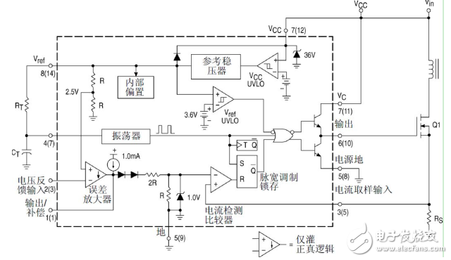
Figure 2 UC3842 internal schematic diagram
As can be seen from the figure, the UC3842 has a total of 8 pins, and the functions of each pin are:
Pin 1 is the output of the error amplifier, and the external resistor-capacitor is used to improve the gain and frequency characteristics of the error amplifier;
The 2 pin is the feedback voltage input terminal, and the voltage of the pin is compared with the 2.5V reference voltage of the non-inverting terminal of the error amplifier to generate an error voltage, thereby controlling the pulse width;
Pin 3 is the current detection input terminal. When the detection voltage exceeds 1V, the pulse width is reduced to make the power supply in intermittent operation;
The 4th pin is the timing terminal, and the operating frequency of the internal oscillator is determined by the external resistance time constant.
f=1.72/(RT&TImes;CT);
5 feet are public ground;
The 6-pin is a push-pull output terminal, and the inside is a totem pole type. The rising and falling time is only 50 ns and the driving capability is ±1 A;
7 feet is the DC power supply terminal, with under- and over-voltage lockout function, the chip power consumption is 15mW;
Pin 8 is a 5V reference output with 50mA load capability. There are two control loops inside the UC3842. One sampling voltage is fed back to the error amplifier. The error amplification voltage signal is generated compared with the reference voltage of 2.5V. One is the sampling voltage generated by the transformer primary current on the sampling resistor Rs, and the output voltage of the error amplifier. The pulse signal of the modulated PWM is compared. Since the error signal actually controls the magnitude of the primary peak current, the UC3842 is a current-mode PWM modulator.
Figure 3 UC3842 working sequence diagram
Figure 3 is a timing diagram when the UC3842 is operating. The charge and discharge waveform generated by RT and CT becomes a square wave signal after being shaped by the oscillator. When charging, the oscillator outputs a low level and is discharged at a high level. During CT charging, the RS flip-flop sets the pin S=“0â€. If the voltage on the sampling resistor Rs is lower than the output winding feedback compensation output voltage (via the error amplifier), the RS flip-flop reset pin R=“0â€. At this time Q
Output low level “0â€, UC3842 output high level Q1 turn-on; when the sampling resistor voltage is higher than the feedback compensation output voltage, RS flip-flop reset R=“1â€, the flip-flop flips, Q
After the output high level "1" passes the OR gate, the UC3842 outputs a low level and Q1 turns off. After the cutoff, the sampling resistor voltage is lower than the output winding feedback compensation output voltage, and the RS flip-flop resets R=“0â€. At this time, the flip-flop is in the output hold state, and Q1 is still off.
When the CT starts to discharge, the RS flip-flop sets the pin S=“1â€. At this time, the trigger is set, then Q outputs a low level “0â€, but after the OR gate, the OR gate output is “1â€. When Q1 is still closed.
When the next state of charge starts, the RS flip-flop sets the pin S=“0â€, and R is also “0†at this time. The flip-flop keeps the output state, Q
The low level “0†is output, and after passing the OR gate, Q1 starts to conduct. Through the description of the normal working state of the above UC3842, it can be seen that the current sampling resistor voltage and the output winding feedback voltage together determine the Q1 switching state.
British Standard Gang Switch And Socket
British Standard Gang Switch And Socket,Standard Gang Switch And Socket,Standard Gang Switch,Standard Gang Switch For Sale
ZHEJIANG HUAYAN ELECTRIC CO.,LTD , https://www.huayanelectric.com