When the circuit board is reflowed, it is easy to cause the plate to bend, and if it is serious, it may even cause the components to be welded, tombstone, etc. How to overcome it?
1. The damage of PCB circuit board deformation
On automated surface mount lines, if the board is not flat, it will cause misalignment, components can not be inserted or attached to the board's holes and surface mount pads, and even the automatic inserter will be damaged. The board on which the components are mounted is bent after soldering, and the component legs are difficult to trim. The board can't be installed in the chassis or the socket inside the machine, so it is very troublesome for the assembly factory to encounter the board. The current surface mount technology is moving toward high precision, high speed, and intelligent direction, which puts higher flatness requirements on PCB boards as homes for various components.
In the IPC standard, it is specifically pointed out that the maximum allowable deformation of a PCB board with a surface mount device is 0.75%, and the maximum allowable deformation of a PCB without a surface mount is 1.5%. In fact, in order to meet the needs of high-precision and high-speed placement, some electronic assembly manufacturers have stricter requirements on the amount of deformation.
The PCB board is composed of copper foil, resin, glass cloth and other materials. The physical and chemical properties of each material are different. When pressed together, thermal stress remains inevitably, resulting in deformation. At the same time, in the processing of PCB, it will undergo various processes such as high temperature, mechanical cutting and wet processing, which will also have an important impact on the deformation of the board. In short, the causes of PCB board deformation are complicated and diverse, how to reduce or eliminate the material characteristics. Different or processing-induced deformations have become one of the most complex problems faced by PCB manufacturers.
2. Analysis of the causes of deformation
The deformation of PCB board needs to be studied from several aspects such as material, structure, pattern distribution and processing process. This paper will analyze and expound various reasons and improvement methods that may cause deformation.
The uneven copper surface area on the board will deteriorate the board bend and the board curl.
Generally, a large area of ​​copper foil is designed for grounding. Sometimes the Vcc layer is also designed with a large area of ​​copper foil. When these large areas of copper foil are not evenly distributed on the same board. When it is on, it will cause the problem of uneven heat absorption and heat dissipation. The circuit board will of course also expand and contract. If the expansion and contraction cannot cause different stresses and deformation at the same time, the temperature of the board will have reached this time. At the upper end of the Tg value, the board begins to soften, causing permanent deformation.
The junctions (vias) of the various layers on the board limit the board's shrinkage
Most of today's circuit boards are multi-layer boards, and there are joints (vias) to the rivets between the layers. The connection points are divided into through holes, blind holes and buried holes. Where there are joints, the board is limited. The effect of rising and contracting will indirectly cause the plate to bend and the plate to be warped.
The weight of the board itself will cause the board to be deformed
In general, the reflow oven uses a chain to drive the board forward in the reflow oven, that is, the two sides of the board are used as fulcrums to support the entire board. If the board has heavy parts or the size of the board is too large, It will show the phenomenon of the middle depression due to its own quantity, causing the plate to bend.
The depth of the V-Cut and the connecting strip will affect the deformation of the panel.
Basically, V-Cut is the culprit in destroying the structure of the board. Because V-Cut cuts the groove on the original sheet, the V-Cut is prone to deformation.
2.1 Analysis of the deformation of the plate by pressing materials, structures and figures
The PCB board is formed by pressing a core board and a prepreg and an outer layer copper foil, wherein the core board and the copper foil are thermally deformed when pressed, and the amount of deformation depends on the coefficient of thermal expansion (CTE) of the two materials.
The coefficient of thermal expansion (CTE) of copper foil is around
The ordinary FR-4 substrate has a Z-direction CTE at the Tg point;
Above TG point is (250~350) X10-6, X-direction CTE is similar to copper foil due to the presence of glass cloth.
Notes on TG points:
High Tg printed board When the temperature rises to a certain area, the substrate will change from "glass state" to "rubber state", and the temperature at this time is called the glass transition temperature (Tg) of the board. That is, Tg is the highest temperature (°C) at which the substrate remains rigid. That is to say, the ordinary PCB substrate material not only softens, deforms, melts, etc. at high temperatures, but also exhibits a sharp drop in mechanical and electrical properties.
Generally, the Tg plate is 130 degrees or more, the high Tg is generally greater than 170 degrees, and the medium Tg is greater than about 150 degrees.
A PCB printed board with a typical Tg ≥ 170 ° C is called a high Tg printed board.
The Tg of the substrate is improved, and the characteristics of heat resistance, moisture resistance, chemical resistance, and stability of the printed board are improved and improved. The higher the TG value, the better the temperature resistance of the sheet, especially in the lead-free process, the high Tg application is more.
High Tg refers to high heat resistance. With the rapid development of the electronics industry, especially the electronic products represented by computers, the development of high functionality and high multi-layer requires the higher heat resistance of PCB substrate materials as an important guarantee. The emergence and development of high-density mounting technology represented by SMT and CMT makes PCBs more and more inseparable from the high heat resistance of substrates in terms of small aperture, fine wiring and thinning.
Therefore, the difference between general FR-4 and high Tg FR-4 is that it is in the hot state, especially under heat absorption, the mechanical strength, dimensional stability, adhesion, water absorption, thermal decomposition of the material. There are differences in various conditions such as thermal expansion, and high Tg products are obviously better than ordinary PCB substrate materials.
The expansion of the core plate in which the inner layer pattern is made is different due to the difference in the pattern distribution and the thickness of the core sheet or the material characteristics. When the pattern distribution is different from the thickness or material characteristics of the core sheet, when the pattern distribution is relatively uniform, the material types are uniform, Will produce deformation. When the PCB board laminate structure is asymmetrical or the pattern distribution is uneven, the CTE difference of different core boards will be large, and deformation will occur during the pressing process. The deformation mechanism can be explained by the following principle.
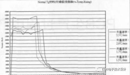
Figure 1 ordinary semi-solid sheet dynamic viscosity curve
It is assumed that there are two kinds of core plates with different CTE differences, which are pressed together by a prepreg, wherein the C core of the A core plate is 1.5×10⁻⁵/° C., and the length of the core plate is 1000 mm. In the press-forming process as a prepreg of the bonding sheet, the two core sheets are bonded together by softening, flowing and filling the pattern, and curing in three stages.
Figure 1 shows the dynamic adhesion bottom curve of ordinary FR-4 resin at different heating rates. Under normal circumstances, the material starts to flow from about 90 °C, and begins to crosslink and solidify when it reaches above TG point. The prepreg is in a free state before curing. At this time, the core plate and the copper foil are in a state of being freely expanded after being heated, and the amount of deformation can be obtained by the respective CTE and temperature change values.
Simulated press conditions, the temperature is raised from 30 ° C to 180 ° C,
At this time, the deformation amounts of the two core plates are respectively
△LA=(180°C~30°C)x1.5x10-5m/°CX1000mm=2.25mm
△ LB = (180 ° C ~ 30 ° C) X2.5X10-5M / ° CX1000mm = 3.75mm
At this time, since the semi-cure is still in a free state, the two core plates are long and short, and do not interfere with each other, and deformation has not yet occurred.
See Figure 2, when pressed, it will be kept at high temperature for a period of time until the semi-curing is completely cured. At this time, the resin becomes solidified and cannot flow freely. The two core plates are combined. When the temperature drops, such as no interlayer When the resin is restrained, the core plate will return to the original length without deformation, but in fact, the two core plates are bonded by the cured resin at a high temperature, and cannot be freely contracted during the cooling process, wherein the A core plate should shrink 3.75. Mm, in fact, when the shrinkage is greater than 2.25mm, it will be hindered by the A core plate. In order to achieve the balance between the two core plates, the B core plate cannot shrink to 3.75mm, and the A core plate shrinks more than 2.25mm, thus making the whole The plate is bent toward the B core plate as shown in Fig. 2.
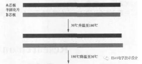
Figure 2 shows the deformation during the pressing process of different CTE core plates
According to the above analysis, the laminated structure and material type of the PCB have been uniformly distributed, which directly affects the difference in CTE between different core plates and copper foil. The difference in shrinkage during the pressing process will pass through the solid film of the prepreg. The process is retained and eventually forms a deformation of the PCB board.
2.2 Deformation caused during PCB processing
The causes of deformation of the PCB board process are very complicated and can be divided into two stresses: thermal stress and mechanical stress. The thermal stress is mainly generated during the pressing process, and the mechanical stress mainly occurs during the stacking, handling and baking of the plates. The following is a brief discussion in the order of the process.
CCL material: CCL is double-sided, symmetrical structure, no pattern, copper foil and glass cloth CTE are almost the same, so there is almost no deformation caused by different CTE during the pressing process. However, the size of the CCL press is large, and there is a temperature difference in different areas of the hot plate, which may cause slight differences in the curing speed and degree of the resin in different regions during the pressing process, and the dynamic viscosity at different heating rates also has a large difference, so it also occurs. Local stress due to differences in the curing process. Generally, this stress will maintain equilibrium after pressing, but will gradually release deformation during processing in the future.
Pressing: The PCB pressing process is the main process for generating thermal stress. The deformation due to different materials or structures is shown in the previous section. Similar to the clad copper clad, it also produces local stress caused by the difference in the curing process. Due to thicker thickness, various pattern distribution, and more prepreg, the thermal stress is more difficult to eliminate than the clad laminate. The stress existing in the PCB is released in subsequent drilling, contouring or grilling processes, resulting in deformation of the panel.
Soldering, character and other baking processes: Since the solder resist inks cannot be stacked on each other when cured, the PCB board will be placed on the shelf and cured by a baking sheet. The soldering temperature is about 150 °C, just above the Tg point of the medium and low Tg material, Tg Above the point, the resin is in a high elastic state, and the plate is easily deformed under the action of its own weight or oven strong wind.
Hot air solder leveling: The normal temperature of the hot plate solder is 225 ° C ~ 265 ° C, the time is 3S-6S. The hot air temperature is 280 ° C ~ 300 ° C. When the solder is leveled, the plate is fed into the tin furnace from room temperature, and then subjected to room temperature post-treatment water washing within two minutes after the furnace is discharged. The entire hot air solder leveling process is a quenching and quenching process. Due to the different materials of the circuit board and the uneven structure, thermal stress will inevitably occur during the hot and cold process, resulting in microscopic strain and overall deformation.
Storage: The storage of the PCB in the semi-finished stage is generally inserted in the shelf. The loose adjustment of the shelf is not suitable, or the stacking of the board during storage will cause mechanical deformation of the panel. Especially for thin plates below 2.0mm, the impact is even more serious.
In addition to the above factors, there are many factors that affect PCB deformation.
3. Improve countermeasures
How can we prevent the board from going through the reflow oven and causing the plate to bend and the board to be warped?
1. Reduce the effect of temperature on the stress of the board
Since "temperature" is the main source of stress in the board, as long as the temperature of the reflow furnace is lowered or the temperature of the board is raised and cooled in the reflow furnace, the bending and warping of the board can be greatly reduced. But there may be other side effects.
2. Use high Tg plate
Tg is the glass transition temperature, that is, the temperature at which the material changes from a glass state to a rubber state. The lower the Tg value, the faster the board starts to soften after entering the reflow oven, and the time to become soft rubbery state. It will also become longer, and the deformation of the board will of course become more serious. The use of a higher Tg sheet can increase its ability to withstand stress and deformation, but the price of the material is relatively high.
3. Increase the thickness of the board
In order to achieve a lighter and thinner purpose, many electronic products have a thickness of 1.0mm, 0.8mm, or even a thickness of 0.6mm. Such a thickness is such that it is difficult to keep the board from deforming after passing through the reflow furnace. It is recommended that if there is no thin and light requirement, the board should preferably use a thickness of 1.6mm, which can greatly reduce the risk of bending and deformation of the board.
4. Reduce the size of the board and reduce the number of boards
Since most reflow ovens use chains to drive the board forward, the larger the size of the board will be deformed in the reflow oven due to its own weight, so try to place the long side of the board as a board edge. On the chain of the reflow furnace, the deformation of the sag caused by the weight of the circuit board itself can be reduced, and the number of the slabs is also reduced for this reason, that is to say, when the furnace is over, the narrow side is used to cross the furnace direction as much as possible, and the minimum can be achieved. The amount of deformation of the depression.
5. Use the oven tray fixture
If the above methods are difficult to achieve, the last step is to use a reflow carrier/template to reduce the amount of deformation. The reason why the over-tray can reduce the bending of the plate is because whether it is thermal expansion or contraction, it is hoped. The tray can hold the board until the temperature of the board is lower than the Tg value and then harden again, and the size of the garden can be maintained.
If the single-layer tray can not reduce the deformation of the circuit board, it is necessary to add a layer of cover to clamp the circuit board with the upper and lower layers of the tray, so that the problem of deformation of the circuit board over the reflow furnace can be greatly reduced. However, this oven tray is quite expensive, and it has to be manually placed to place and recycle the tray.
6. Use solid connection, stamp hole instead of V-Cut
Since V-Cut will destroy the structural strength of the board between boards, try not to use the V-Cut board or reduce the depth of the V-Cut.
Optimization in PCB production engineering:
Influence of different materials on the deformation of plates
The deformation rate of different material plates was exceeded and the defect rate was counted. The results are shown in Table 1.
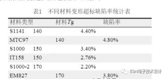
It can be seen from the table that the low Tg material deformation defect rate is higher than the high Tg material. The high Tg materials listed in the above table are filler-shaped materials, the CTE is smaller than the low Tg material, and during the processing after pressing, The baking temperature is up to 150 ° C, and the effect on low Tg materials will definitely be greater than the medium and high Tg materials.
Engineering design research
Engineering design should avoid structural asymmetry, material asymmetry, and graphic asymmetry to reduce the occurrence of deformation. At the same time, it is found that the direct compression structure of the core plate is more easily deformed than the copper foil compression structure. Table 2 shows Test results of two structural panels.
It can be seen from Table 2 that the defect rate of the two structural deformations is obviously different. It can be understood that the core plate pressing structure is composed of three core plates, and the expansion and contraction between the different core plates and the stress changes are more complicated and more difficult to eliminate. .

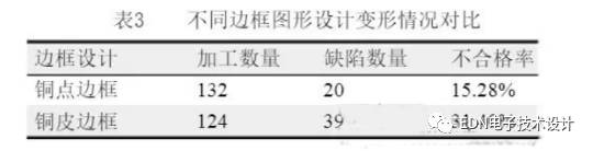
In engineering design, the layout of the panel has a great influence on the deformation. In general, the PCB factory will have a continuous large copper border and a discontinuous copper or copper frame, and there are also different differences.
Table 3 shows the comparison test results of the two frame design panels. The reason why the deformation of the two kinds of frame forms is different is because the continuous copper frame has high strength, and the rigidity is relatively large during the process of pressing and splicing, so that the residual stress in the plate is not easily released, and is concentrated after the shape is processed and released. Causes deformation to be more serious. Instead of a continuous copper dot frame, the stress is gradually released during the pressing and subsequent processing, and the deformation of the single plate is small after the shape.
The above are some of the possible influencing factors involved in engineering design, such as the flexibility to use in design. It can reduce the effects of deformation caused by design.
3.3 Pressing study
The effect of press-fitting on deformation is essential, and the generation of stress can be effectively reduced by reasonable parameter setting, press selection and lamination. For general structurally symmetrical plates, it is generally necessary to pay attention to the symmetric stacking of the plates when pressing, and to symmetrically place auxiliary tools such as tool plates and cushioning materials. At the same time, the selection of cold and hot integrated press press is also helpful to reduce thermal stress. The reason is that the hot and cold split presses transfer the plate to the cold press at high temperature (above GT temperature), and the material loses pressure above the Tg point. Rapid cooling will cause rapid release of thermal stress and deformation, while the cold and hot integrated press can reduce the temperature at the end of hot pressing to avoid the loss of pressure of the plate at high temperature.
At the same time, for the special needs of customers, there will inevitably be some materials or structurally asymmetrical plates. At this time, the deformation caused by the different CTEs will be very obvious. For this problem, we can try to use asymmetric The stacking method is to solve the problem, the principle is that the asymmetric placement of the buffer material reaches the double-sided heating speed of the PCB board, thereby affecting the expansion and contraction of different CTE core cypress trees in the heating and cooling stages to solve the problem of inconsistent deformation. Table 4 shows the test results on a certain structural asymmetrical plate of our company.
Through the asymmetric stacking method, as well as increasing the post-cure process after pressing, and leveling before shipment, the board finally meets the customer's 2.0mm requirements.
3.4 Other production processes
In the PCB production process, in addition to the press-fit, there are several high-temperature treatment processes of solder mask, characterization and hot air leveling. Among them, the maximum temperature of the soldering plate after the solder mask and the character is 150 ° C. The temperature mentioned above is in the ordinary Tg material. Above the Tg point, the material is in a high elastic state and is easily deformed under external force. Therefore, it is necessary to prevent the lower plate from being bent when the plate is baked, and to ensure that the direction of the plate is parallel to the blowing direction when the plate is baked. In the hot air leveling process, it is necessary to ensure that the plate is discharged from the tin furnace for more than 30 seconds, so as to avoid quenching deformation caused by cold water washing after high temperature treatment.
In addition to the production process, the storage of PCB boards in various stations also has a certain impact on the deformation. In some manufacturers, due to the large number of production and the narrow space, multiple boards will be stacked and stored together, which will also lead to the board. The parts are deformed by external force, and since the PCB board also has certain plasticity, these deformations will not be 100% restored in the subsequent leveling process.
3.5 Leveling before shipment
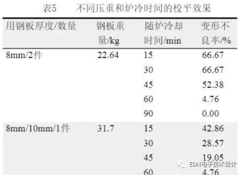
Most PCB manufacturers have a leveling process before shipment, because in the process of processing, it will inevitably produce deformation of the plate caused by heat or mechanical force, and can be leveled by mechanical leveling or hot-baked before shipment. Get effective improvement. Under the influence of heat resistance of the solder resist and the surface coating layer, the general baking plate temperature is below 140 ° C ~ 150 ° C, just beyond the Tg temperature of ordinary materials, which has great advantages for the leveling of ordinary plates, and for high Tg materials. The leveling effect is not so obvious, so the temperature of the baking sheet can be appropriately increased on the high Tg plate with severe individual plate warpage, but the main ink and coating quality. At the same time, the method of pressing the weight and increasing the cooling time with the furnace also has a certain improvement effect on the deformation. Table 5 shows the test results of the different levels of pressure and furnace cooling time on the leveling of the plate, from which it can be seen that the weight is increased. And extending the furnace cooling time has a significant effect on the leveling of the deformation.
Stainless Steel Black Leather Rod
Stainless Steel Black Leather Rod, 304 Stainless Steel Round Bar, Stainless Steel Flat Bar, Stainless Steel Threaded Rod
ShenZhen Haofa Metal Precision Parts Technology Co., Ltd. , https://www.haofametal.com