Abstract: Based on a brief introduction of DMA controller core 2837, this paper presents the interface circuit with single chip microcomputer 8031.
In some single-chip application systems, it is often necessary to solve the problem of rapidly transferring data between an external device and a storage reservoir. To this end, this paper studies the interface technology between DMA controller 8237 and microcontroller 8031.
1, 8237 chip introduction 1.1 structureThe DMA controller 8237 is provided with three basic control logic blocks. It includes timing control logic block, program command control block and priority coding logic block; there are four direct transmission channels. Each channel has a base address register (16 bits), a base byte counter (16 bits), a current address register (16 bits), and a current byte counter (16 bits), and each channel has a 6-bit Mode register. In addition, the 8237 data lead and address lead have a tristate buffer. It can take over or release the bus.
Main pin of 1·2 8237CLK (clock signal, input), CS (chip select signal, input), HLDA (CPU response signal to 8237 request, input), DREQ0~DREQ3) DMA request signal, input), DB0~DB7 (data bus, input / Output), IOW (I/O write signal, input/output), IOR (I/O read signal, input/output), EOP (process end signal, input/output), A0~A3 (address code, input/output) ), A4 - A7 (address code, output), MEMR (memory read signal, output), MEMW (memory write signal, output), HRQ (request signal sent by the DMA controller 8237 to the CPU, output), DACK0~DACK3 (DMA response signal, output), ADSTB (address strobe signal, output).
1.3 main function register life
Let the register format:
The command register is an 8-bit register that is used to control the operation of the 8237. The contents are assigned by the microcontroller in the programming state, and the port address is osH.
The meaning of everyone is as follows:
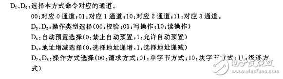
D0: Controls whether memory to memory transfer is allowed. D0=0 is allowed, D0=1 is not allowed
D1: When the memory to memory transfer mode is selected, the address of the control channel o remains unchanged. D1=O does not allow the channel O address to remain unchanged, D1=1 allows the channel. The address remains the same.
D2: Control whether the DMA controller is allowed to work, D2=0 allows DMA operation, D2=1 does not allow DMA operation.
D3: Select the working timing. D3=O normal timing, D3=1 compression timing (this bit has no effect when D3=1)
D4: Select the priority method. D4 = O fixed priority, D4 = 1 cycle priority.
D5: Select bus cycle write command timing. D5=o delayed write, D5=1 extended write
D6: Select the active level of the DREQ signal. D6=0DREQ is active high, D6=1DREQ is active low.
D7: Select the active level of the DACK signal. D7=0DACK is active low. D7=1DACK is active high.
Mode register format:
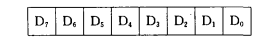
Each channel has a mode register that controls the DMA transfer mode of a channel. The port address is OBH
The meaning of everyone is as follows:
The system structure is shown in Figure 1:
Angled Finish Nail,Resists Moisture Nail,Hardware Angled Finish Staple,Reliable 0.087 Inch Nail
Zhejiang Best Nail Industrial Co., Ltd. , https://www.beststaple.com