The core idea of ​​digital substation is equipment intelligence, information interaction, control network, function integration, state visualization, and ultimately achieve a strong and reliable smart grid. Compared with traditional substations, digital substations add a powerful process layer service unit between the bay level and the primary equipment, which can connect existing primary equipment to the digital substation. The main equipment in the process layer is the intelligent interface unit: including the circuit breaker operation box and the knife gate interface control box. This paper introduces the realization of the knife gate interface control box.
The knife gate interface box is used to control the isolating switch, and its reliability becomes a key part of the digital station maintenance. Therefore, it is necessary to design a high-reliability device to prevent the load pulling and closing switch, the grounding switch with the grounding, and the grounding wire (grounding). Knife brake) combined circuit breaker (isolation switch). The device also needs to meet intelligent control and communication to ensure compliance with the IEC61850 standard. This paper introduces the design method of high reliability and communication control of the knife gate interface box by using dual FPGA.
1 system designA 220 kV circuit breaker requires 7 isolating knife gates, and one isolating knife gate requires 6 switching volume collection points and 1 group of interlocking combination contacts. The six switching quantities are used to acquire the opening and closing position information of the three-phase knife gate. In addition to the above functions, the knife gate interface control box also has signal indicator control, multiple self-test functions, communication control, field status signal acquisition and upload, superior control command reception, analysis, execution, etc. The functional block diagram is shown in Figure 1. Shown. In order to achieve high reliability control, dual FPGA control is adopted logically. Independent double start is adopted on the drive circuit, and the multi-relay "logic and" combination is used to realize the exit control. Prevent accidental closing of the isolating switch during the inspection of the knife gate, resulting in personal injury or death.
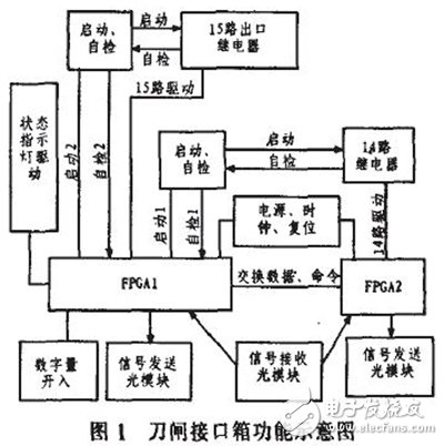
The digital input is used to collect the on-site signal status and the logic control hard pressure plate. The opening circuit has certain anti-interference ability; the exit circuit has 7-way opening, 7-way closing and 7-way blocking for executing the corresponding circuit points. Gate and closing. Both the inlet and outlet have strong and weak electrical isolation loops, which can guarantee the 4-level fast transient and surge level 4 immunity test. The optical transceiver channel is used for realizing remote control, realizing on-site data and device status quantity uploading and receiving control commands, and realizing the knife gate splitting operation. There are also 14 indicators to indicate the opening and closing position and the operating status of the unit. The device also has a CPU unit for data operations and parsing execution commands. The CPU unit exchanges data with the first FPGA through the serial port, and exchanges data and commands with the second FPGA through the GPIO. The two FPGAs are independently activated and exported; the exit relay contacts are then logically combined to achieve a higher level of reliable transmission. The exit self-test loop includes start self-test, breakdown self-test and disconnection self-test. Among them, the startup and disconnection faults immediately alarm, and the outlet is immediately blocked when the breakdown occurs. The core of the hardware design is two identical FPGAs. All the logic functions of the device are realized by using these two FPGA chips. The chip uses XILINX's XC3S50AN, with 50k system gates, 1 584 logic cells, 1 MbitFlashROM, 65 KRAM, 3 multipliers, 2 DCM clock managers; up to 144 IO ports. The chip also features low power consumption and flexible signal level compatibility; the core 1.2 V, IO 3.3 VTTL support 5 V tolerant input. The PU unit adopts a unit with serial port and GPIO. It is not introduced here. The focus of this solution is to adopt advanced export self-test, start-up and export logic combination; FPGA system design: power management, reset circuit, clock distribution and FPGA configuration Circuit design.
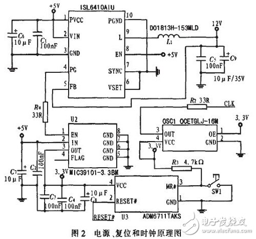
1.2 Power supply, reset and clock system designThis device requires the following power supplies: 24 V power supply for the output relay, 5 V power supply for the optical signal transceiver module, 3.3 V power supply for the FPGA IO, clock circuit to provide the drive power, 1.2 V for the FPGA core Provide working power. The maintenance-free LAMDA power module HWS50/HD is used to convert DC 220 V to +24 V; the DC-DC module PSS3—24-5 converts +24 V to +5 V. The 3.3 V and 1.2 V required by the FPGA use the high-efficiency power management chip ISL6410AIU and MIC39101-3.3BM. The implementation method is shown in Figure 2. The U1-4 pin is the 1.2 V power supply completion flag. Use this signal to control the 3.3 V power supply of the U2-1 pin to ensure that the core power supply is working reliably before establishing the IO power. L1 is a filter inductor, which should ensure the flow capacity of the load. The model of DO1813H-153MLD from Coalcraft is used. The high-reliability integrated circuit ADM6711TAKS is used to implement manual reset and level threshold monitoring reset. The reset output signal PORESET# is active low, ensuring a reliable reset of the entire system. Echoll's high-precision low-temperature drift crystal oscillator OCETGLJ-16 M is used. The required power supply is 3.3 V and the output clock is 16 MHz. It is connected to the global clock input of the FPGA and can directly drive two FPGAs.
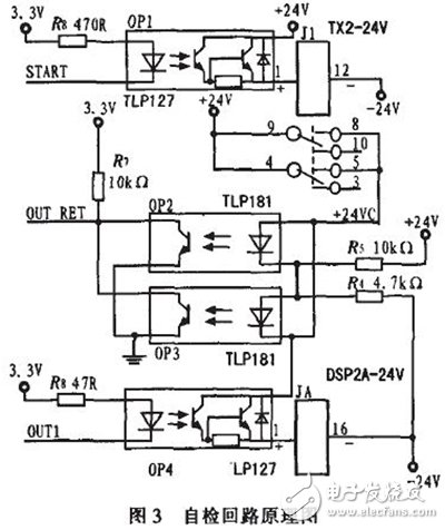
In order to realize the outlet blocking, an exit starting circuit is designed, and the signal can be opened only when the outlet circuit and the starting circuit operate simultaneously. In order to prevent circuit failure and cause rejection, the self-test circuit designed for the start and exit circuits is shown in Figure 3. Each of the two FPGAs has a complete set of start-up and self-test loops, and the combined exit is realized by using two FPGA-driven relay contacts for "logical AND". Start self-test method: turn off the exit signal (OUT1 high level), turn on the start relay (START low level); OP1 turns on, J1 action +24VC turns on 24 V power supply, OP2 turns on, OUT_RET goes low, Implement a self-test. Exit self-test method: turn off the start relay (START high level), open the outlet (OUT1 low level); OP3, OP4 turn on, OUT_ RET goes low, realize the exit loop self-test. When the multi-channel exit self-test, each line needs to be self-tested in turn. Since there may be interference, it can be determined by setting a 10-wheel self-test error of a certain road.
Uv Curving Screen Protector,Uv Curl Screen Protector,Uv Screen Protector Tempered Glass,Anti Uv Computer Screen Protector
Shenzhen TUOLI Electronic Technology Co., Ltd. , https://www.hydrogelprotectors.com