As field-programmable gate array (FPGA) chips become more widely used in commercial, military, aerospace and other fields, reliability and testability are particularly important. The use of FPGAs is quite flexible for designers. However, it is the uncertainty and reprogrammability of this application that increases the difficulty of chip testing. At present, more work has been focused on the research of FPGA test methods based on SRAM structure [1-7]. The core question is what kind of test model to build, and what kind of test stimuli to apply to activate the fault, and at the same time, it can be measured at the reach. Therefore, it is also necessary to determine where to apply the stimulus and where to take the measurement.
According to requirements, FPGA testing can be divided into manufacturing-oriented test process (MT P) and application-oriented test process (AT P). The MT P is mainly tested from the manufacturer's point of view, and the test cost is mainly reflected in the cost of the test time determined by the length of the test vector set. MTP is primarily tested for programmable logic blocks (CLBs), input and output units (IOBs), programmable wiring (PI), and SRAM for programming. AT P is a test at the application level, that is, the FPGA is configured to test for specific functions. It is highly targeted and the test process is relatively simple. However, whether it is MTP or AT P, there is at least one process of {Test Configuration (TC), Vector Implementation (TS)} [6]. Complete testing often requires repeated configuration and testing. In general, programming is time consuming and the programming configuration is slow. Therefore, the key to FPGA testing is how to combine FPGA low-speed online configuration and high-speed testing with a minimum number of programming times to ensure complete coverage.
This paper introduces a test programming method based on SRAM structure FPGA logic resources, and takes Xilinx's XC4000 series [8] as an example, on the BC3192V50 digital-analog hybrid integrated circuit test system, through the serial mode, data configuration and testing .
2 FPGA based on SRAM structureFrom the programming principle, FPGAs are mainly based on two types of anti-fuse (arrTIfuse) structure and SRAM-based structure. The XC4000 series is based on the SRAM structure. The logic function is configured based on the SRAM structure of the internal array distribution. The different logic functions of these SRAMs are used to determine the logic functions of each part. It can also be implemented by loading different configuration data. The logic function is constantly updated and repeatedly rewritten. In fact, the configuration data loaded on the SRAM determines and controls the logical functions and connections between the various CLBs, IOBs, and PIs. Another important feature of FPGAs based on SRAM architecture is the so-called Logical Element Array (LCA) architecture. It is this LCA distribution structure that combines the dual features of gate arrays and programmable devices. The LCA acts like a gate array, interconnecting the programmable logic blocks as required by the internal programmable wiring to implement the logic functions in the array.
In addition, thanks to advanced semiconductor processes and improved architecture, the XC4000E Series is capable of supporting system clock frequencies up to 80 MHz and internal performance in excess of 150 MHz.
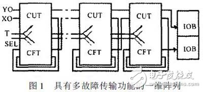
3 test programmingBy programming, the CLBs of each row are connected to form a one-dimensional array [1-2]; each array is tested as a whole, as shown in Figure 1.
The fault model uses a multi-CLB hybrid fault model, that is, multiple logic units can fail in one FPGA, and faults in logic units use different fault models for different circuits. For a lookup table structure, it is assumed that it can have a fixed fault fixed at "0" or "1"; for multiplexers and triggers, it is assumed that various functional faults can occur [4-5].
The CLB in each array is programmed as shown in Figure 1. The output signal of the previous CLB acts as the input signal for the next CLB, and only the CLBs at the left and right ends are connected to the IOB. All CLBs are designed to be programmed to the same circuit structure, both the circuit under test (CUT) and the fault transfer circuit (CFT). The two lookup tables G and F in the CLB are designed with one fault active end (T), two fault transfer ends (Yn and Xn) and one fault transfer mode selector
The four-input logic structure of (SEL) uses the same T input and SEL inputs. The two inputs (Yn and Xn) of lookup table F are connected to the outputs (QYn and QXn) of the two flip-flops in this CLB to detect and pass the fault signal of the flip-flop. Look for the two output signals (Yn and Xn) of tables G and F as the input signals (Yn+ 1 and Xn+ 1) of lookup table G in the next CLB.
The fault transfer circuit uses a circuit form based on AND gates and OR gates [4]. Use the SEL input to control whether the gate is transmitted or the gate is transmitted. At this time, if there is one or more CLB input and output terminals with fault information of normal 1 ( 0) and error 0 ( 1), fault information 0 ( 1) can always be observed at the output end.
Testing all arrays in parallel reduces test time and required IOB. At the same time, because all CLBs have the same programming structure, clock and vertical inputs can be shared, and inputs from different arrays can be shared, further reducing the required IOB [ 1-2].
However, since the programmed array is a timing array, the time required to test the array is increased to some extent. On the other hand, since each CLB is used to transmit fault information while being tested, the test accuracy is reduced compared to the method of transmitting fault information by a single line of CLBs [3-5].
Uv Curing Hydroge Film,Uv Protective Curing Film,Flexible Uv Curing Film,Uv Hydrogel Curing Film
Shenzhen TUOLI Electronic Technology Co., Ltd. , https://www.szhydrogelprotector.com