Nowadays, high-intensity gas discharge lamps have been widely used in squares, road lighting and other occasions due to their high luminous efficiency, good color temperature and long life. Among them, metal halide lamps are considered to be one of the best artificial light sources because of their many advantages. However, due to the negative resistance characteristics of metal halide lamps and special starting requirements, they must be used in conjunction with matching ballasts. Compared with traditional inductive ballasts, electronic ballasts have many advantages, and its research and development is also a hot spot in the power electronics industry.
In order to ensure that the metal halide lamp does not exhibit acoustic resonance, the electronic ballast generally operates in a low frequency square wave state. The traditional low frequency square wave electronic ballast includes a three-stage structure: a power factor correction circuit, a step-down circuit, and a full-bridge inverter circuit. This structure is very complicated and causes the cost of the ballast to be expensive. Simplifying circuits and reducing costs have become the focus of today's research. One method is to combine the first two stages of power factor correction and step-down circuits. This method can reduce the volume of the ballast, but the accompanying problem is that the performance of the power factor correction circuit is reduced, and the stress of the switching device is increased. Another method is to combine the step-down circuit and the inverter circuit. This method can reduce the size and cost of the ballast, but the control method can be relatively complicated.
A combination of a step-down circuit and a half-bridge inverter circuit is a popular and feasible method. Because this type of circuit is relatively simple and the lowest cost. In order to promote the wide application of this scheme, simplify its control method, overcome the shortcomings of this circuit, and improve its reliability has become the focus of research.
In this paper, a new control method is proposed for this kind of circuit, and a simple and effective method is proposed to overcome the current overshoot problem caused by the commutation of the output current and reduce the peak coefficient.
1 circuit description
The block diagram of the circuit is shown in Figure 1.
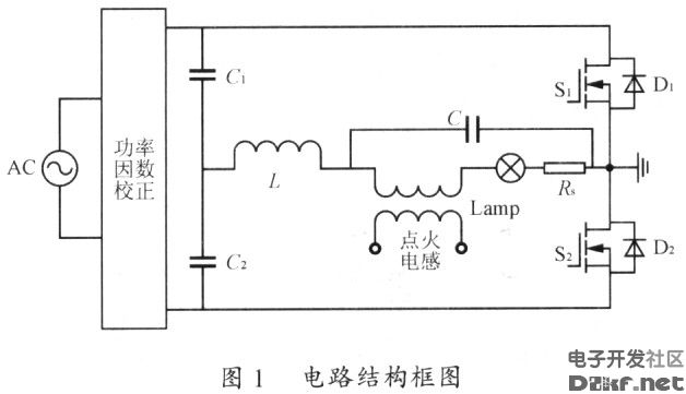
1.l Analysis of circuit working mode
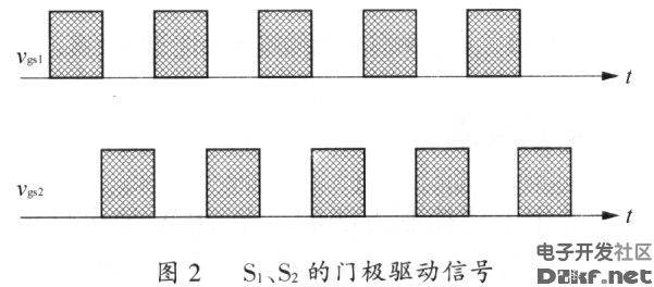
The gate signals of S1 and S2 are shown in Fig. 2. When S1 is operating in the high frequency state, S2 is turned off. At this point, the circuit is equivalent to a Buck circuit, S1 is equivalent to the main power switch, and the body diode of S2 is equivalent to the Buck diode. The operating state of the two switching tubes alternates at a frequency of 400 Hz. In this way, a low frequency square wave current output supply lamp can be obtained.
There is a reverse recovery problem when the diode is turned off, which greatly increases the switching loss of the device. In order to avoid this, we let the circuit work in the current interrupted state. Figure 3 is a schematic diagram of the state of the inverter stage inductor current.
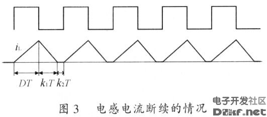
When S1 is operating in the high frequency state and S2 is off, the circuit operates in three operating modes.
1.ll mode 1
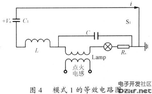
S1 is turned on, current flows through C1, S1, Rs, lamp, ignition inductance, and Lc. Figure 4 is an equivalent circuit diagram of this mode. The inductance of the ignition inductor is much smaller than the inductance of the inductor L. It is assumed that the voltage on the capacitor C remains constant during each switching cycle, and the voltage VL on the inductor L is

L.1.2 Mode 2
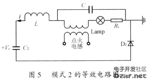
S1 is disconnected. Since the inductor current cannot be abrupt, current flows through Rs, lamp, ignition inductance, L, C2, and D2o. Figure 5 is an equivalent circuit diagram of this mode. The voltage of the inductor L is

1.1.3 mode 3
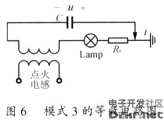
S1 is still in the disconnected state. But the current of the inductor £ is zero. At this point, capacitor C supplies energy to the lamp, and current flows through C, Rs, the lamp, and the ignition inductance. Figure 6 is an equivalent circuit diagram of this mode of operation. Assuming that the capacitance is large enough and the voltage across the capacitor remains the same, we can get the output lamp voltage from equations (1) and (2).

Where: the coefficient k1 is related to the inductor current drop time, which is clearly indicated in Figure 3.
When S1 is turned off and S2 is operated in the high frequency switching state, the working process of the circuit is basically consistent with the above analysis.
According to the above analysis, the half-bridge inverter circuit can be equivalent to a Buck step-down circuit in every half of the low frequency period. Thus, a half-bridge inverter circuit can provide a suitable T voltage for the lamp and enable the lamp to operate in a low frequency square wave state.
1.2 closed loop control
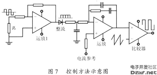
Because of the negative resistance of the metal halide lamp, for this reason we control the output of the ballast as a characteristic of the current source to ensure the stable operation of the lamp. Fig. 7 is a block diagram showing a control method of a half bridge circuit. The lamp current is sampled by Rs. The voltage across the sampling resistor Rs is a low frequency square wave signal. First, the signal is amplified by the operational amplifier l, and then the AC square wave signal is rectified into a direct current through a rectifying circuit, and then subjected to RC filtering to perform PI adjustment, and the output is adjusted to be a constant current source. It can be seen that this control method is equivalent to the DC/DC control method and is simple and effective.
1.3 Current overshoot
However, a serious problem with this circuit is that there is a large current overshoot at the moment of commutation of each output current. Such spike currents can greatly reduce lamp life. This paper presents a simple and effective way to overcome this problem.
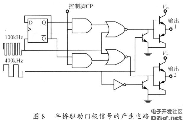
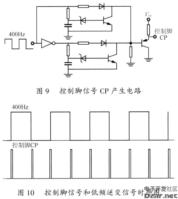
Figure 8 is a half-bridge drive gate signal generation circuit in which a D flip-flop, two AND gates, and two NOR gates are combined to reduce the duty cycle of the drive signal. This function is controlled by the control pin (CP). When CP is high, the duty cycle of the drive can be reduced to about half of the original. In this way, we can give CP a high level at the moment of commutation of each output current, reducing the duty cycle of the drive to greatly reduce or even eliminate the overshoot current. Figure 9 shows the production of a simple CP control signal. Figure 10 is a timing diagram of the foot CP signal and the low frequency inverter signal.
2 Experimental results
A 70W metal halide lamp electronic ballast prototype using the above control method has been completed. The main parameters of the circuit are as follows.
L="380" μH;
C = 1 μF;
Vo="200V";
Fh="100" kHz;
F1=400Hz.
Where: fh is the high frequency and low frequency frequency driven by the half bridge circuit;
F1 is the low frequency frequency driven by the half bridge circuit.
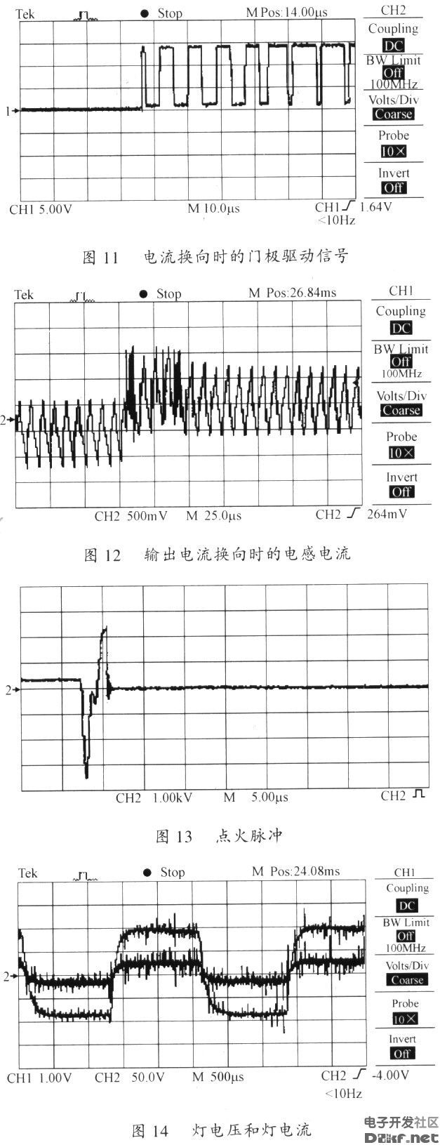
Figure 11 shows the change in the drive signal when the output current is commutated. Figure 12 shows the change in inductor current when the output current is commutated. It can be seen that the overshoot of the current is quite small. Figure 13 shows the ignition pulse. Since the ignition is performed at a low frequency, the ignition success rate is high. Figure 14 shows the current and voltage waveforms during normal lamp operation. It can be seen that the lamp current has substantially no current overshoot. The overall efficiency is about 90% and the crest factor is 1.1.
3 Conclusion
This paper presents a new control method for two-stage low-frequency square wave metal halide lamp electronic ballast. It regulates the output as a constant current source to ensure stable operation of the lamp. At the same time, the current overshoot problem existing in the circuit is overcome. Compared with the traditional 3-level low-frequency square wave electronic ballast, this circuit and control method is simple and effective, so-called cheap and good.
Smart Bms,Bms For Battery,Bms For Lithium Battery,Bms Module
HuiZhou Superpower Technology Co.,Ltd. , https://www.spchargers.com